Semiconductor device

a technology of semiconductor devices and diodes, which is applied in the direction of semiconductor devices, solid-state devices, transistors, etc., can solve the problems of inability to accurately determine the polarity of output current, the risk of forward voltage increasing in the diode device region, and the inability to fix voltage in a configuration, so as to reduce forward voltage and forward voltage. , the effect of reducing losses

Active Publication Date: 2018-10-25
DENSO CORP
View PDF0 Cites 13 Cited by
  • Summary
  • Abstract
  • Description
  • Claims
  • Application Information

AI Technical Summary

Benefits of technology

The present invention is about a semiconductor device that improves recovery characteristics and reduces forward voltage in all current ranges. It reduces loss of efficiency due to increased forward voltage when it is not possible to determine the operation mode. This results in a more efficient semiconductor device and reduced power consumption.

Problems solved by technology

However, in a configuration where the polarities of the output current switch over in short cycles as in an inverter circuit, there may be a current range where determination of polarities of the output current cannot be made accurately depending on the tolerances of current sensors.
However, the voltage cannot be fixed in a configuration where a negative voltage is applied to the diode device region depending on the polarity of the output current.
Thus, the inventors have found the problem of the risk that the forward voltage may increase in the diode device region.
When it is not determinable whether the operation mode is the reverse conduction mode or the forward conduction mode, an increase of saturation voltage across the collector and emitter of the IGBT device is limited, since, even if the operation mode is actually the forward conduction mode, the output current of the IGBT device is small enough in a current range where the mode determination is not possible.

Method used


Image

  • Semiconductor device
  • Semiconductor device
  • Semiconductor device

Examples


first embodiment

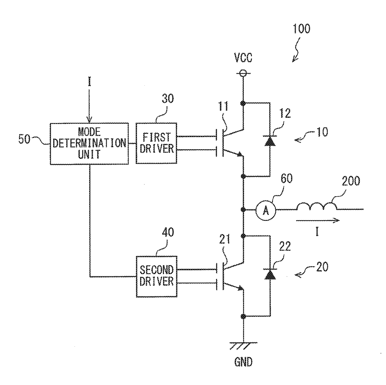
[0023]First, the schematic configuration of a semiconductor device according to the present embodiment will be described with reference to FIG. 1.

[0024]In the present embodiment, a reverse conducting insulated-gate bipolar transistor (RC-IGBT), having a diode device and an insulated-gate bipolar transistor (IGBT) device on the same semiconductor substrate, will be described.

[0025]The RC-IGBT is applied to an inverter, which is a semiconductor device.

[0026]As shown in FIG. 1, the inverter 100 includes two reverse conducting insulated-gate bipolar transistors 10 and 20, drivers 30 and 40 for applying gate voltage to gate electrodes of the reverse conducting insulated-gate bipolar transistors 10 and 20, respectively, and a mode determination unit 50 that determines the driving state of each of the reverse conducting insulated-gate bipolar transistors 10 and 20.

[0027]As shown in FIG. 1, the inverter 100 is configured to have the two reverse conducting insulated-gate bipolar transistors ...

second embodiment

[0082]In addition to the reverse conducting insulated-gate bipolar transistors that are the first device 10 and second device 20 described in the first embodiment, there is preferably also pillar regions 79 having n-type conductivities as shown in FIG. 8. The pillar regions 79 are formed so as to extend from the second main surface 70b of the semiconductor substrate 70 in the thickness direction, through the anode region 76a or body region 76b, and to reach the first barrier region 75a and second barrier region 75b. The pillar regions 79 are a diffusion layer where impurities of the same conduction type as that of the first and second barrier regions 75a and 75b are doped. Thus the pillar regions 79 and barrier regions 75a and 75b have substantially the same potential.

[0083]With the pillar regions 79 provided, when forward bias is applied across the anode electrode 78 and the cathode electrode 71, the anode electrode 78 is short-circuited to the pillar regions 79 via the metal-semic...

third embodiment

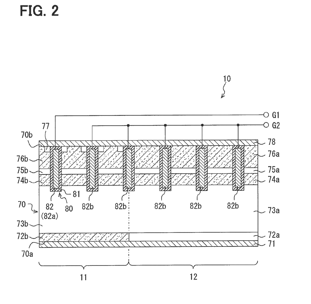
[0087]The thinned-out structure mentioned in the description of the planar layout with reference to FIG. 3 in the first embodiment will be described more specifically in the present embodiment. The present embodiment adopts the aspect with pillar regions 79 described in the second embodiment. As shown in FIG. 9, the gate electrodes 82 adjacent each other are not short-circuited to the anode electrodes 78 in the diode device 12. In other words, gate electrodes 82 adjacent the gate electrodes 82 short-circuited to the anode electrodes 78 are assigned as the second gate electrodes 82b. The first barrier regions 75a formed in the diode device 12 are in contact with at least one second gate electrode 82b via the insulating film 81, so that the diode device 12 can provide the effect of reducing the forward voltage VF by application of the negative voltage −V2 to the second gate electrodes 82b. Also, the effect of reducing the gate capacitance by the thinned-out structure can be achieved.

[...


PUM


Abstract

A semiconductor device includes: reverse conducting switching elements-in each of which a diode element and a switching element are arranged in parallel on a single semiconductor substrate; a driver applying a gate voltage to a plurality of gate electrodes in the reverse conducting switching elements; and a mode determination unit determining whether a forward conduction mode in which a current mainly flows through the switching element or a reverse conduction mode in which the current flows through the diode element is being operated.

Description

CROSS REFERENCE TO RELATED APPLICATION[0001]This application is a U.S. national stage application of International Application No. PCT / JP2016 / 087505 filed on Dec. 16, 2016 and is based on Japanese Patent Application No. 2016-13713 filed on Jan. 27, 2016, the disclosures of which are incorporated herein by reference.TECHNICAL FIELD[0002]The present disclosure relates to a semiconductor device equipped with a switching device and a reverse conducting diode.BACKGROUND[0003]As described in Patent Literature 1, a semiconductor device having a reverse conducting insulated-gate bipolar transistor (RC-IGBT) is known. In the semiconductor device, a negative voltage is applied to an insulated trench gate electrode when an IGBT device region is switched off and circulating current flows to a diode device region.[0004]The semiconductor device allegedly allows holes flowing out from an anode region to be readily injected to a drift layer along the insulated trench gate electrode, whereby the for...

Claims


Application Information

Patent Timeline
IPC IPC(8): H01L21/8234H01L27/06H01L29/739H01L29/78H01L29/868H01L27/088
CPCH01L21/823418H01L27/06H01L29/739H01L29/78H01L29/868H01L27/088H01L29/861H01L29/407H01L29/87H02M1/08H02M7/003H02M7/538H01L27/0727H01L29/7397H01L29/0834H01L29/4238H01L29/0696H01L29/083H01L29/7805H01L29/1095H01L29/0623H01L29/7802
Inventor KAKIMOTO, NORIYUKI
Owner DENSO CORP
Why Eureka
Try Eureka