Process Monitoring Of Deep Structures With X-Ray Scatterometry

a deep structure and process monitoring technology, applied in the field of metalrology systems and methods, can solve the problems of difficult optical radiation penetration to the bottom layer, difficult characterization, and increased measurement difficulty, and achieve the effect of greater precision and certainty of measured parameters and length of measurement tim

Active Publication Date: 2018-12-06
KLA TENCOR TECH CORP
View PDF2 Cites 20 Cited by
  • Summary
  • Abstract
  • Description
  • Claims
  • Application Information

AI Technical Summary

Benefits of technology

[0024]The measurement frequency of a particular high aspect ratio structure under fabrication depends on the stability of the monitored process parameter. Moreover, the length of measurement time required depends on the scattering sensitivity to changes in the monitored process variable. Measuring a scattering signal in-situ provides the fastest measurement of process conditions but with the highest degree of uncertainty. Whereas, longer measurement times provide greater precision and certainty of the measured parameters. In general, process parameters that affect the entire scattering volume (e.g., etch time) can be monitored the fastest, while other parameters (e.g., minor deviations of the etch profile) require either a moving average or longer measurement time to achieve meaningful results. Thus, these parameters can only be controlled on a slower basis.

Problems solved by technology

As devices (e.g., logic and memory devices) move toward smaller nanometer-scale dimensions, characterization becomes more difficult.
Devices incorporating complex three-dimensional geometry and materials with diverse physical properties contribute to characterization difficulty.
For example, modern memory structures are often high-aspect ratio, three-dimensional structures that make it difficult for optical radiation to penetrate to the bottom layers.
Optical metrology tools utilizing infrared to visible light can penetrate many layers of translucent materials, but longer wavelengths that provide good depth of penetration do not provide sufficient sensitivity to small anomalies.
As a result, the parameters characterizing the target often cannot be reliably decoupled with available measurements.
However, the mirror like structure of 3D FLASH intrinsically causes decreasing light intensity as the illumination propagates deeper into the film stack.
This causes sensitivity loss and correlation issues at depth.
In this scenario, optical SCD is only able to successfully extract a reduced set of metrology dimensions with high sensitivity and low correlation.
Optical radiation is often unable to penetrate layers constructed of these materials.
As a result, measurements with thin-film scatterometry tools such as ellipsometers or reflectometers are becoming increasingly challenging.
However, these approaches have not reliably overcome fundamental challenges associated with measurement of many advanced targets (e.g., complex 3D structures, structures smaller than 10 nm, structures employing opaque materials) and measurement applications (e.g., line edge roughness and line width roughness measurements).
Optical methods may provide non-destructive tracking of process variable between process steps, but regular calibration by destructive methods is required to maintain accuracy in the face of process drift, which optical methods cannot independently distinguish.
Atomic force microscopes (AFM) and scanning-tunneling microscopes (STM) are able to achieve atomic resolution, but they can only probe the surface of the specimen.
In addition, AFM and STM microscopes require long scanning times. Scanning electron microscopes (SEM) achieve intermediate resolution levels, but are unable to penetrate structures to sufficient depth.
Thus, high-aspect ratio holes are not characterized well.
In addition, the required charging of the specimen has an adverse effect on imaging performance.
X-ray reflectometers also suffer from penetration issues that limit their effectiveness when measuring high aspect ratio structures.
For example, transmission electron microscopes (TEM) achieve high resolution levels and are able to probe arbitrary depths, but TEM requires destructive sectioning of the specimen.
But, these techniques require sample destruction and lengthy process times. The complexity and time to complete these types of measurements introduces large inaccuracies due to drift of etching and metrology steps because the measurement results become available long after the process has been completed on the wafer under measurement.
Thus, the measurement results are subject to biases from further processing and delayed feedback.
In addition, these techniques require numerous iterations which introduce registration errors.
In summary, device yield is negatively impacted by long and destructive sample preparation required for SEM and TEM techniques.
For processes undertaken in vacuum, this causes significant delay.
As a result, SA metrology systems cannot provide fast measurement feedback to process tools, particularly process tools involving vacuum.
Current in-situ sensors are only capable of monitoring bulk changes to film thicknesses and do not correlate well to the complex profiles that result from the processing of deep 3-D structures.
However, the inability to measured parameters of interest of high aspect ratio structures in a cost effective and timely manner results in low yield, particularly in the memory sector of a wafer.
In summary, ongoing reductions in feature size and increased depth of many semiconductor structures imposes difficult requirements on metrology systems, including stand-alone systems and those integrated with process tools, such as ion implant and etch tools.
Thus, these parameters can only be controlled on a slower basis.

Method used


Image

  • Process Monitoring Of Deep Structures With X-Ray Scatterometry
  • Process Monitoring Of Deep Structures With X-Ray Scatterometry
  • Process Monitoring Of Deep Structures With X-Ray Scatterometry

Examples


Embodiment Construction

[0043]Reference will now be made in detail to background examples and some embodiments of the invention, examples of which are illustrated in the accompanying drawings.

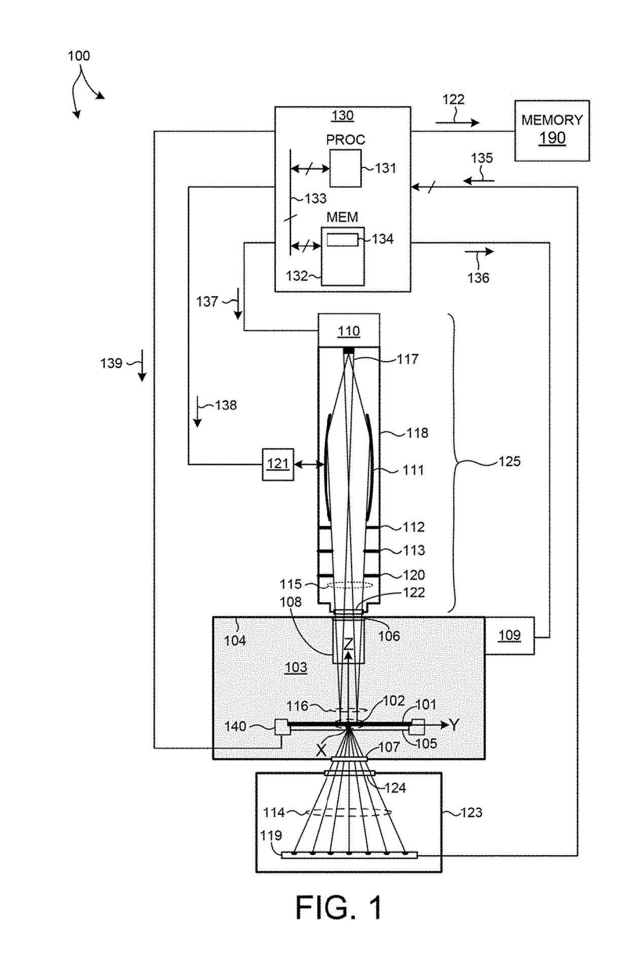
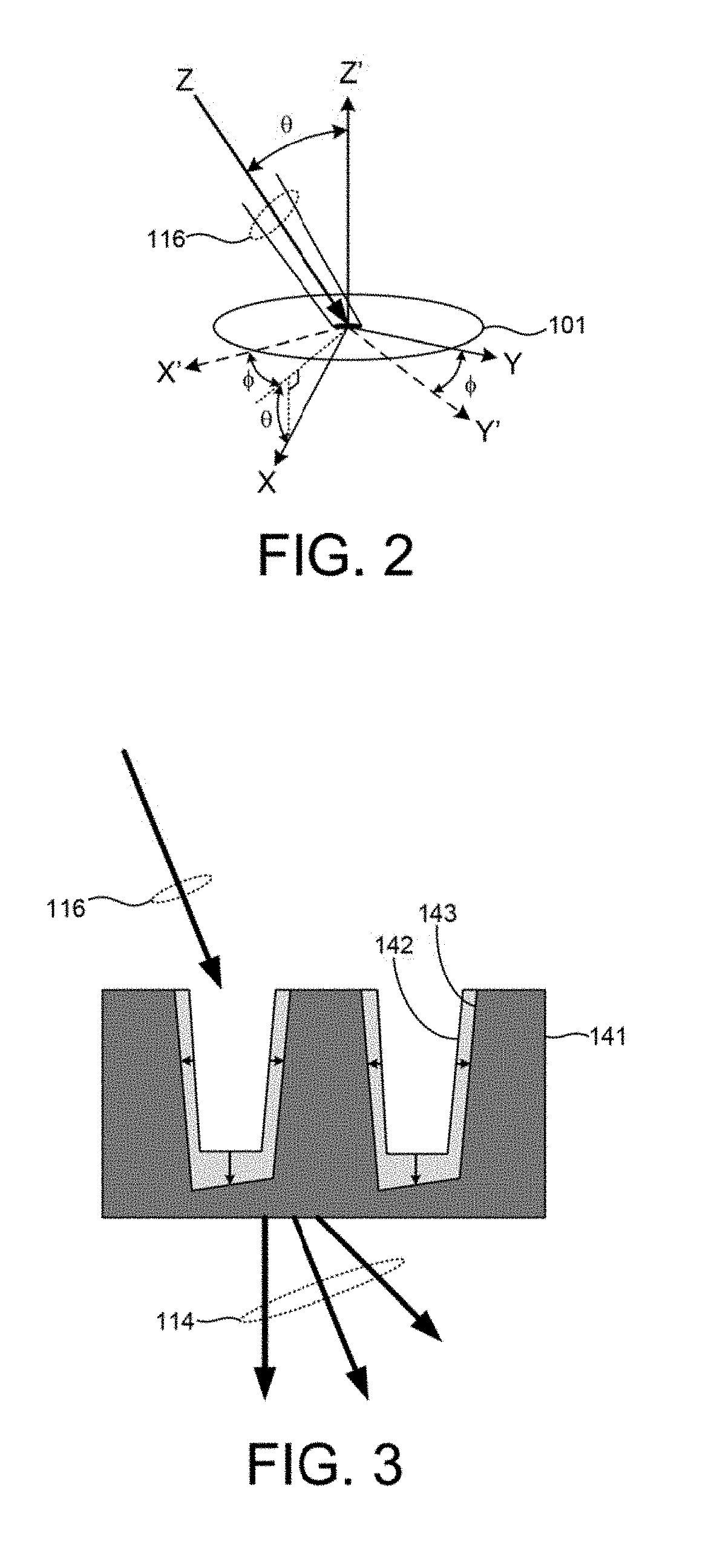
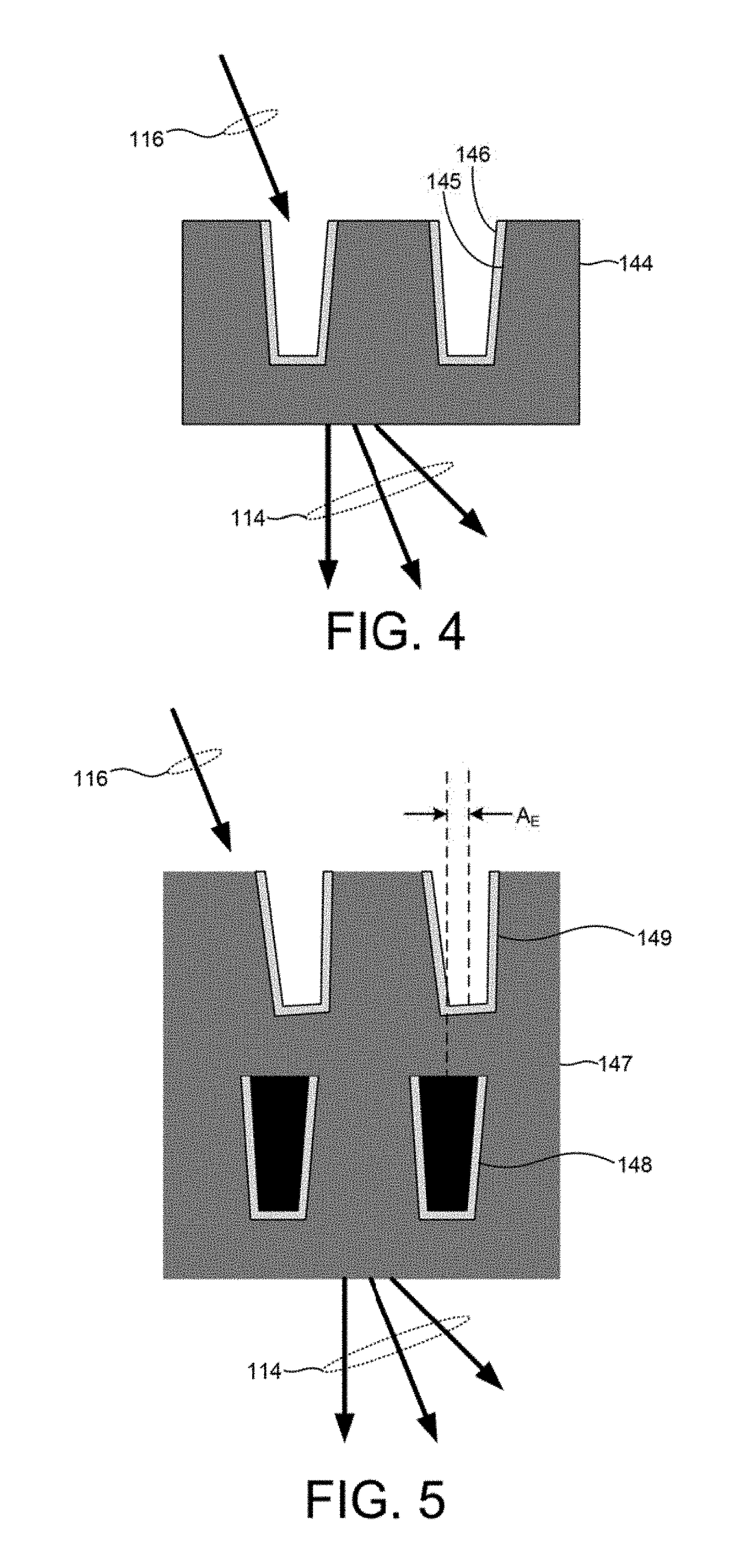
[0044]Methods and systems for estimating values of process parameters, structural parameters, or both, based on x-ray scatterometry measurements of partially fabricated, high aspect ratio semiconductor structures are presented herein. X-ray scatterometry measurements of high aspect ratio structures are performed at one or more steps of a fabrication process flow. Exemplary process steps include etch, deposition, and lithography processes. The measurements are performed quickly and with sufficient accuracy to enable yield improvement of an on-going semiconductor fabrication process flow. In some examples, measurements performed while the wafer is being processed are used to control the on-going process. High aspect ratio structures include sufficient overall scattering volume and material contrast to efficiently scatte...


PUM

PropertyMeasurementUnit
roughnessaaaaaaaaaa
wavelengthsaaaaaaaaaa

Abstract

Methods and systems for estimating values of process parameters, structural parameters, or both, based on x-ray scatterometry measurements of high aspect ratio semiconductor structures are presented herein. X-ray scatterometry measurements are performed at one or more steps of a fabrication process flow. The measurements are performed quickly and with sufficient accuracy to enable yield improvement of an on-going semiconductor fabrication process flow. Process corrections are determined based on the measured values of parameters of interest and the corrections are communicated to the process tool to change one or more process control parameters of the process tool. In some examples, measurements are performed while the wafer is being processed to control the on-going fabrication process step. In some examples, X-ray scatterometry measurements are performed after a particular process step and process control parameters are updated for processing of future devices.

Description

CROSS REFERENCE TO RELATED APPLICATION[0001]The present application for patent claims priority under 35 U.S.C. § 119 from U.S. provisional patent application Ser. No. 62 / 512,297, entitled “Process Monitoring for Deep Structures Using X-Ray Scatterometry,” filed May 30, 2017 and from U.S. provisional patent application Ser. No. 62 / 572,566, entitled “Process Monitoring for Deep Structures Using X-Ray Scatterometry,” filed Oct. 16, 2017, the subject matter of each is incorporated herein by reference in its entirety.TECHNICAL FIELD[0002]The described embodiments relate to metrology systems and methods, and more particularly to methods and systems for improved measurement of semiconductor structures undergoing a fabrication process step.BACKGROUND INFORMATION[0003]Semiconductor devices such as logic and memory devices are typically fabricated by a sequence of processing steps applied to a specimen. The various features and multiple structural levels of the semiconductor devices are forme...

Claims


Application Information

Patent Timeline
Patent Type & Authority Applications(United States)
IPC IPC(8): H01L21/66G01N23/20H01L21/67
CPCH01L22/20G01N23/20083H01L21/67253G01N2223/6116G03F7/70616H01L22/12G03F7/70525G01N23/201G01B15/00G01N2223/054G01B2210/56
Inventor GELLINEAU, ANTONIO ARIONDZIURA, THADDEUS GERARD
Owner KLA TENCOR TECH CORP
Why Eureka
Try Eureka