

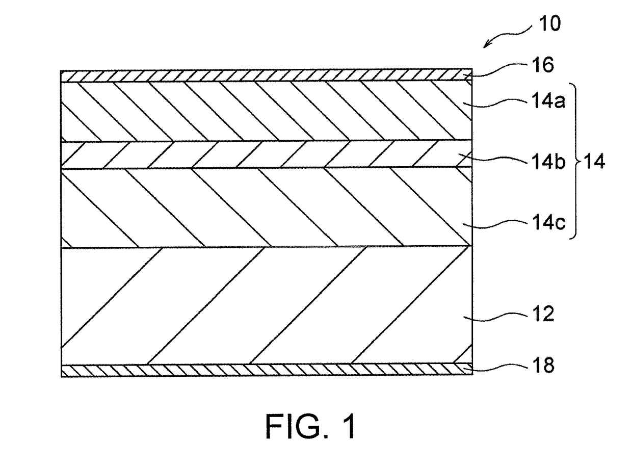
Polycrystalline gallium nitride self-supported substrate and light emitting element using same
a technology of polycrystalline gallium nitride and self-supporting substrate, which is applied in the direction of polycrystalline material growth, chemistry apparatus and processes, crystal growth process, etc., can solve the problems of inability to configure a light emitting device having a vertical structure, high cost, and small area of single crystal substrates in general, and achieve high conversion efficiency, excellent properties, and high luminous efficiency
- Summary
- Abstract
- Description
- Claims
- Application Information
AI Technical Summary
Benefits of technology
Problems solved by technology
Method used
Image

Examples
examples
[0071]The present invention will now be more specifically described by way of the following examples.
example a1
Ge-Doped Self-Supporting Gallium Nitride Substrate
[0072](1) Production of C-Plane Oriented Alumina Sintered Body
[0073](1a) Production of Stack
[0074]Mixed were 100 parts by mass of fine alumina powder (TM-DAR (average particle diameter 0.1 μm), Taimei Chemicals Co., Ltd.), 0.0125 parts by mass (125 mass ppm) of magnesium oxide (500 A, manufactured by Ube Materials Industries, Ltd.), 7.8 parts by mass of poly(vinyl butyral) (product number BM-2, manufactured by Sekisui Chemical Co., Ltd.) as a binder, 3.9 parts by mass of di-(2-ethylhexyl) phthalate (manufactured by Kurogane Kasei Co. Ltd.) as a plasticizer, 2 parts by mass of sorbitan trioleate (Rheodol SP-O30, manufactured by Kao Corporation) as a dispersant, and 2-ethylhexanol as a dispersion medium. The amount of the dispersion medium was adjusted such that the slurry viscosity was 20,000 cP. The resulting slurry was cast onto a sheet into a dry thickness of 40 μm on a PET film by doctor blading to prepare a fine alumina powder la...
example a2
Ge-Doped Self-Supporting Gallium Nitride Substrate
[0108](1) Production of Ge-Doped Self-Supporting Polycrystalline Gallium Nitride Substrate
[0109](1a) Deposition of Seed Crystal Layer
[0110]An oriented Al2O3 substrate was prepared as in Example A1 except that the thickness of the buffer layer was 4 nm and a seed crystal layer was formed by the MOCVD.
[0111](1b) Deposition of Ge-Doped GaN Layer by Na Fluxing
[0112]A Ge-doped GaN layer was formed as in Example A1 except that 0.1 g of Ca was added. In the resulting sample, Ge-doped gallium nitride crystals were deposited on the entire surface of the 60 mm seed crystal substrate, and the crystal thickness was about 1.2 mm. No cracks were observed.
[0113]The oriented alumina substrate portion of the sample prepared in this way was removed by grinding with grinding wheel to yield a Ge-doped gallium nitride single body. The plate surface of the Ge-doped gallium nitride crystals was polished to planarize the plate surface. Furthermore, the plat...
PUM
| Property | Measurement | Unit |
|---|---|---|
| diameter | aaaaa | aaaaa |
| tilt angle | aaaaa | aaaaa |
| tilt angle | aaaaa | aaaaa |
Abstract
Description
Claims
Application Information