

Resin composition, resin film, semiconductor laminate, method for manufacturing semiconductor laminate, and method for manufacturing semiconductor device
a technology of resin film and semiconductor, applied in the direction of synthetic resin layered products, semiconductor/solid-state device details, applications, etc., can solve the problems of warpage influence, peeling between the encapsulant, and substrate bending, so as to improve the adhesion, improve the strength, and reduce the effect of warpag
- Summary
- Abstract
- Description
- Claims
- Application Information
AI Technical Summary
Benefits of technology
Problems solved by technology
Method used
Image


Examples
examples
[0100]Hereinafter, the present invention will be specifically described by showing synthesis Examples, Examples, and Comparative Examples, but the present invention is not limited to the following Examples.
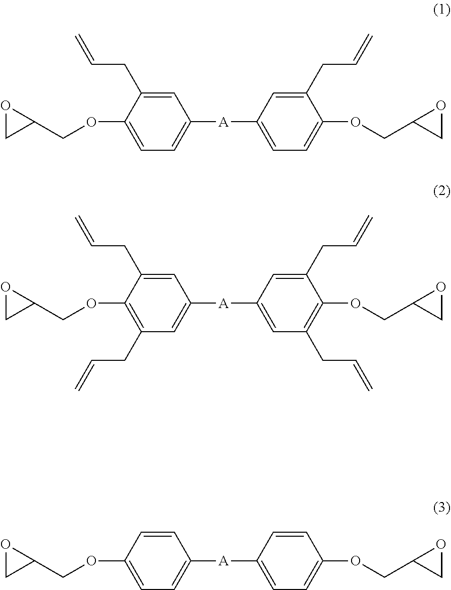
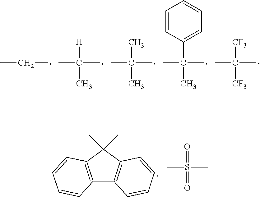
[0101]The following Compounds S-1 to S-8 were used.
Synthesis Example of Epoxy Compound 1
[0102]Into a 5 L flask equipped with a stirrer, a thermometer, a nitrogen inflow instrument, and a reflux condenser, 617 g (2.0 mol) of Compound S-1, 256 g (8.0 mol) of methanol, and 852 g (8.0 mol) of epichlorohydrin were introduced. Then, 768 g (19.2 mol) of sodium hydroxide was added over 2 hours, followed by increasing the temperature to 60° C., and the mixture was allowed to react for 3 hours. After the reaction, 500 mL of toluene was added thereto, and the organic layer was washed with pure water until the water layer became neutral. Subsequently, the solvent in the organic layer was removed under reduced pressure to give 757 g (1.8 mol) of Epoxy compound (1).
Synthesis Example of Epoxy Co...
PUM
| Property | Measurement | Unit |
|---|---|---|
| tensile strength | aaaaa | aaaaa |
| mass % | aaaaa | aaaaa |
| temperature | aaaaa | aaaaa |
Abstract
Description
Claims
Application Information