

Quantum dot device and electronic device
a quantum dot and electronic technology, applied in semiconductor devices, solid-state devices, material nanotechnology, etc., to achieve the effect of improving the performance of the quantum dot devi
- Summary
- Abstract
- Description
- Claims
- Application Information
AI Technical Summary
Benefits of technology
Problems solved by technology
Method used
Image

Examples
synthesis example 1
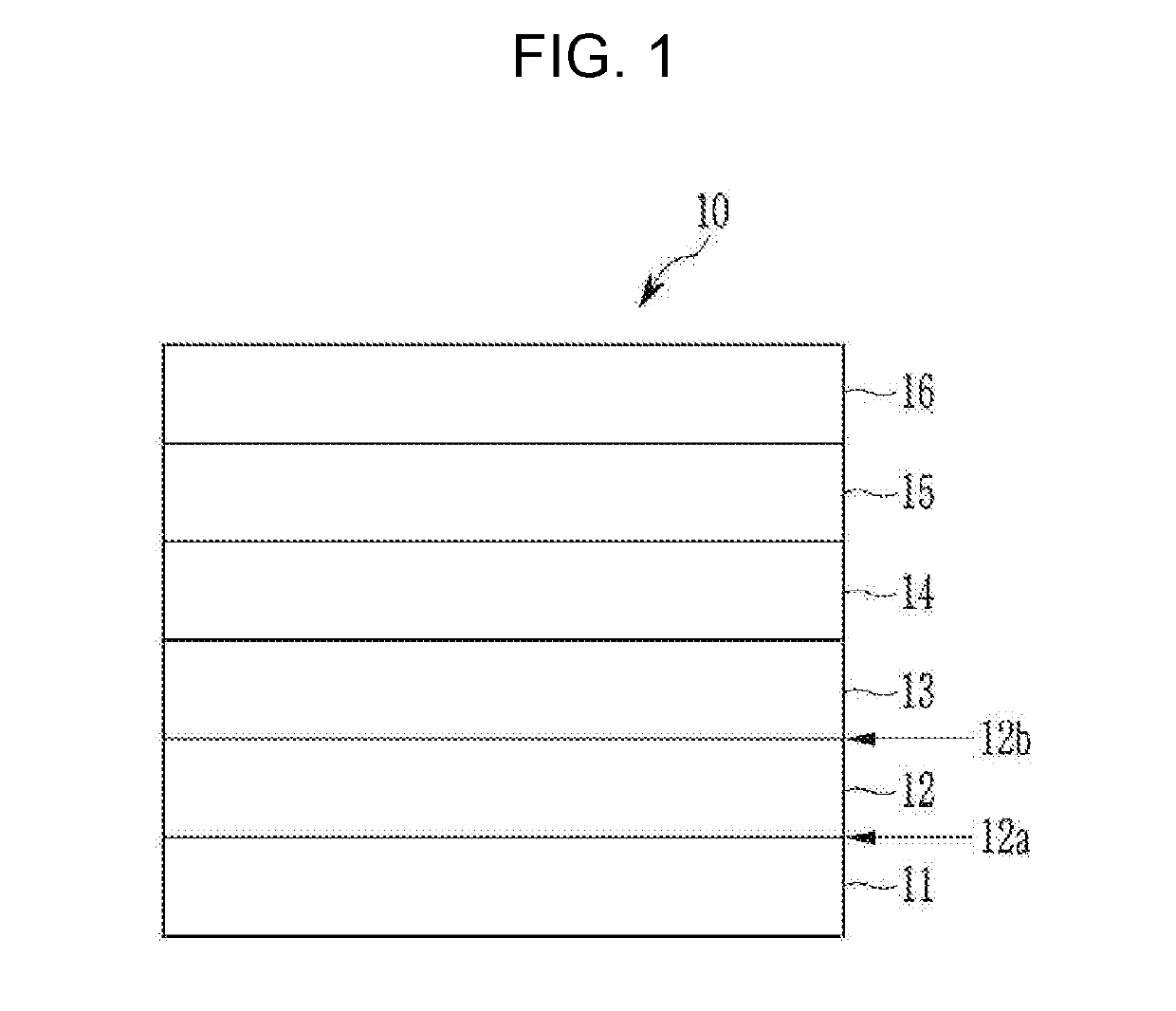
Core
[0163]Selenium (Se) and tellurium (Te) are respectively dispersed in trioctylphosphine (TOP) to prepare a 2 molar (M) Se / TOP stock solution and a 0.1 M Te / TOP stock solution. 0.125 millimoles (mmol) of zinc acetate along with 0.25 mmol of palmitic acid, 0.25 mmol of hexadecyl amine, and 10 milliliters (mL) of trioctylamine is put in a reactor, and the reactor is heated at 120° C. under vacuum. One hour later, an atmosphere in the reactor is converted into nitrogen. After heating the reactor at 300° C., the Se / TOP stock solution and the Te / TOP stock solution in a Te / Se ratio of 1 / 25 is rapidly injected thereinto. Subsequently, acetone is added to the reaction solution rapidly cooled down to room temperature after 10 minutes, 30 minutes, or 60 minutes, and a precipitate centrifuged therefrom is dispersed in toluene to obtain a ZnTeSe quantum dot.
synthesis example 2
m Dot of ZnTeSe Core / ZnSeS Shell
[0164]1.8 mmol (0.336 grams (g)) of zinc acetate, 3.6 mmol (1.134 g) of oleic acid, and 10 mL of trioctylamine are put in a flask and then, vacuum-treated at 120° C. for 10 minutes. Nitrogen (N2) is used to substitute an internal atmosphere of the flask, and the flask is heated up to 180° C. The ZnTeSe core according to Synthesis Example 1 is added thereto within 10 seconds, subsequently, 0.04 mmol of Se / TOP is slowly injected thereinto, and the mixture is heated up to 280° C. Then, 0.01 mmol of S / TOP is added thereto, and the obtained mixture is heated up to 320° C. and reacted for 10 minutes. Subsequently, a mixed solution of 0.02 mmol of Se / TOP and 0.04 mmol of S / TOP is slowly injected thereinto, and the obtained mixture is reacted for 20 minutes again. Then, when a step of injecting a mixed solution by changing a mixing ratio of Se and S and reacting the obtained mixture for 20 minutes is repeated, the mixed solution of Se and S is a mixed solutio...
preparation example 1
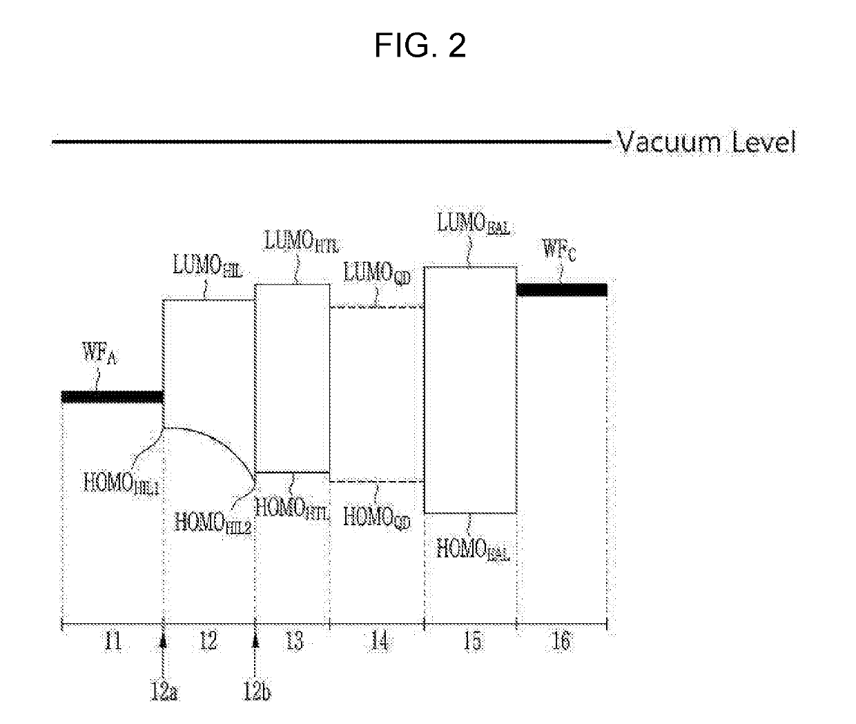
[0165]A solution for a hole injection layer is prepared by mixing a conductive polymer solution ((poly(3,4-ethylenedioxythiophene)polystyrene sulfonate, PEDOT:PSS) (HOMO: 5.3 eV) (Clevios™ A14083, Heraeus Company, 6 parts by weight of PSS based on 1 part by weight of PEDOT) and an insulating polymer solution including a polymer represented by Chemical Formula A (water:alcohol=4.5:5.5 ratio by volume (v / v), 5 weight percent (wt %), Aldrich-Sigma Co., Ltd.) in a weight ratio of 1:1 (a weight ratio of a polymer solute:1:3.6 ratio by weight (w / w)).
PUM
 Abstract
Description
Claims
Application Information