Avalanche Photodetector with Single Mesa Shape

a photodetector and single-mesa technology, applied in the field ofavalanche photodetectors, can solve the problems of power budget becoming the key issue of limiting the maximum transmission capacity, affecting device speed, and affecting device speed, so as to achieve high electric field

Inactive Publication Date: 2019-12-05
NAT CENT UNIV
View PDF0 Cites 5 Cited by
  • Summary
  • Abstract
  • Description
  • Claims
  • Application Information

AI Technical Summary

Benefits of technology

[0007]The main purpose of the present invention is to provide an epitaxial-layers structure with n-side down, where the strongest electric field of an M-layer is coated in inner bottom layers to avoid surface breakdown; a single mesa shape is used to limit the electric field of the M-layer; and all layers are far below breakdown except the M-layer has a particularly high electric field.
[0008]Another purpose of the present invention is to change secondary holes into secondary electrons through p-type-doping an absorption layer, where carriers is made run fast because electrons run fast; junction capacitance is reduced with surface area increased by a depletion layer thickened; and fast response speed is obtained with sensitivity effectively improved.
[0009]Another purpose of the present invention is to thicken an i-layer, use only one absorption layer and add a DBR layer below an n-type ohmic contact layer for acquiring better effects, where the DBR layer is of indium gallium arsenide phosphide / indium phosphide (InGaAsP / InP) or indium aluminum gallium arsenide / indium aluminum arsenide (InAlGaAs / InAlAs).

Problems solved by technology

If the technology of wavelength division multiplexing (WDM) was continued to be used, the insertion loss in passive device would make the power budget become the key issue of limiting the maximum transmission capacity.
When the M-layer was made thin, breakdown might happen at the edge for achieving required operation gain.
However, for reducing the chance of surface breakdown, the excessive edge-field buffer layer 41 and N-charge layer 42 are required, which might result in impact on device speed.
As a result, the ohmic contact might be hard to be produced and the resistance of the whole device is made big.
In addition, the structure also sacrificed the field-limitation of the P-type InGaAs absorption layer 46, where the parasitic capacitance of the device might become bigger.
Nevertheless, because of the stronger fringe field in the absorption layer, the difficulty of packaging the device was increased (F Nakajima, M. Nada, and T. Yoshimatsu, “High-Speed Avalanche Photodiode and High-Sensitivity Receiver Optical Sub-Assembly for 100-Gb / s Ethernet,” to be published in IEEE / OSA Journal of Lightwave Technology, vol.
This could cause reliability problem.
Yet, this made the dark current abruptly rise to deteriorate the sensitivity.
Therefore, the discharging speed of carrier became slower to further affect the output power as the device was made much slower in speed.
Hence, the prior arts do not fulfill all users' requests on actual use.

Method used


Image

  • Avalanche Photodetector with Single Mesa Shape
  • Avalanche Photodetector with Single Mesa Shape
  • Avalanche Photodetector with Single Mesa Shape

Examples


Embodiment Construction

[0018]The following description of the preferred embodiment is provided to understand the features and the structures of the present invention.

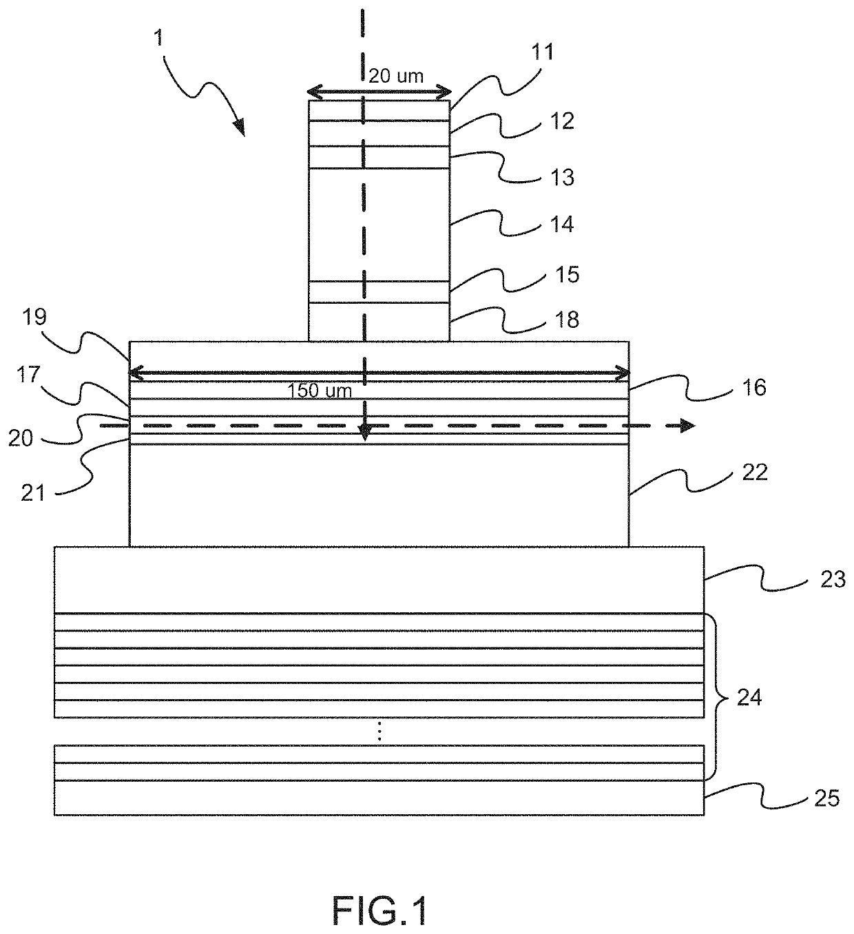
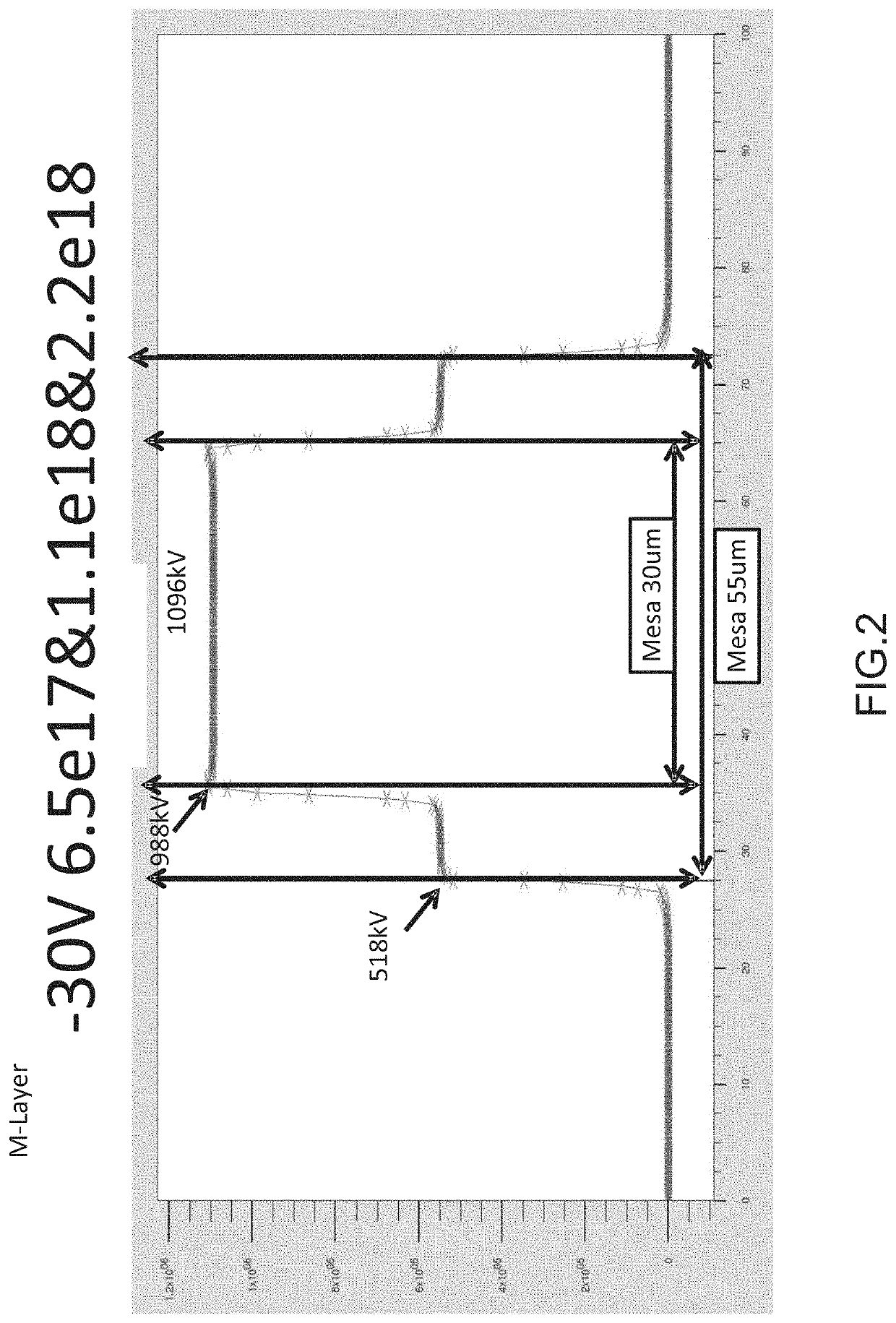
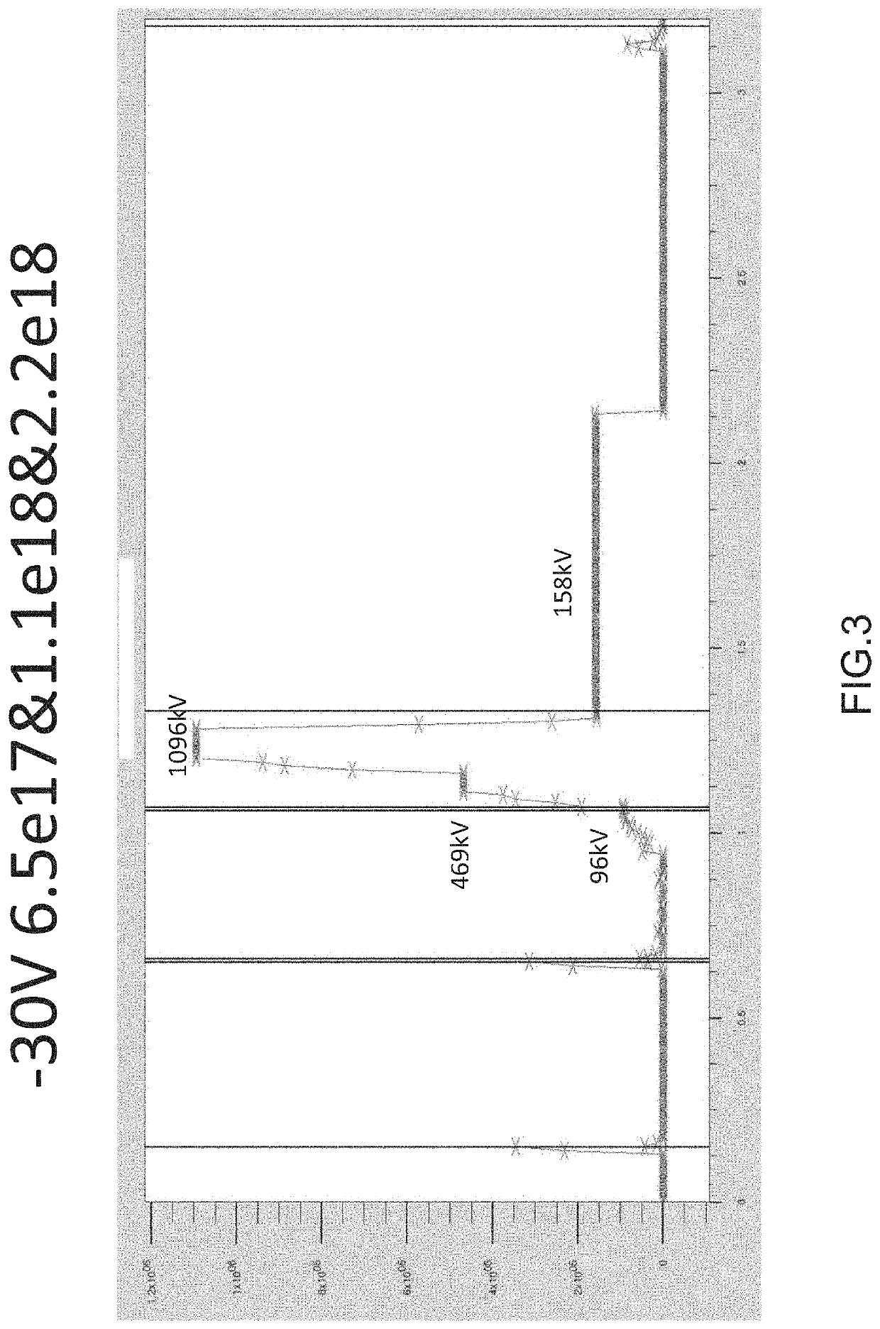
[0019]Please refer to FIG. 1 to FIG. 4, which are a sectional view showing a preferred embodiment according to the present invention; a view showing a two-dimensional distribution of electric field at breakdown; a view showing a one-dimensional distribution of electric field at breakdown; a sectional view showing a state-of-use of the preferred embodiment. As shown in the figures, the present invention is a device of avalanche photodetector having a single mesa shape, comprising a p-type ohmic contact layer 11, a p-type window layer 12, a first graded bandgap layer 13, a p-type absorption layer 14, a second graded bandgap layer 15, a field buffer layer 16, a first p-type field control layer 17, a second p-type field control layer 18, a spacer layer 19, a multiplication layer (M-layer) 20, an n-type field control layer 21, an intrinsic layer (...


PUM


Abstract

A photodetector is provided. The photodetector is an avalanche photodiode of indium aluminum arsenide (InAlAs). An epitaxial-layers structure with n-side down is used. The strongest electric field of a multiplication layer (M-layer) is coated in inner bottom layers to avoid surface breakdown. An intrinsic layer is thickened; only one absorption layer is used; and a DBR layer is added below an n-type ohmic contact layer. A graded bandgap layer is etched to form a single mesa shape. Through the single mesa shape, all layers are far below breakdown except the M-layer has a particularly high electric field for restraining the electric field. Thus, the present invention changes holes into electrons through p-type-doping the absorption layer; because electrons run fast, carriers is made run fast; and junction capacitance is reduced with surface area increased by depletion layer thickened. Consequently, fast response speed is obtained while sensitivity is effectively improved.

Description

TECHNICAL FIELD OF THE INVENTION[0001]The present invention relates to an avalanche photodetector; more particularly, to thickening an intrinsic layer (i-layer), using only one absorption layer (p-type doped) and adding a distributed Bragg reflector (DBR) layer below an n-type ohmic contact layer with a mesa shape etched out, where, through the single mesa shape, a multiplication layer (M-layer) obtains a high electric field at the center of the device along with a low electric field at the edge of the device; the electric field of the M-layer is limited; and all layers are far below breakdown except the M-layer has a particularly high electric field.DESCRIPTION OF THE RELATED ARTS[0002]To meet the much more demands of the internet of things (IOT) for virtual machines using bit data, traditional copper wires have long been unable to take on the transmission tasks (≥˜100 meters (m)). Optical fiber having transmission bandwidth of no bottom still is bound to be the only hope. Under co...

Claims


Application Information

Patent Timeline
Patent Type & Authority Applications(United States)
IPC IPC(8): H01L31/107H01L31/0304H01L31/0232H01L31/0352H01L31/0224
CPCH01L31/1075H01L31/02327H01L31/035281H01L31/022408H01L31/03046
Inventor SHI, JIN-WEI
Owner NAT CENT UNIV
Why Eureka
Try Eureka