Energy storing interposer device and manufacturing method

a technology of interposer and manufacturing method, which is applied in the direction of semiconductor/solid-state device details, material nanotechnology, capacitors, etc., can solve the problems of high-speed integrated circuits that are extremely sensitive to electrical noise, the physical area of defined components is reduced, and the integration of such densely populated dies may come with a price, so as to improve the power management system, increase the number of energy-storing devices, and prolong the life of regular batter

Active Publication Date: 2020-03-19
SMOLTEK AB
View PDF0 Cites 1 Cited by
  • Summary
  • Abstract
  • Description
  • Claims
  • Application Information

AI Technical Summary

Benefits of technology

The present invention is based on the realization that compact local energy storage and / or efficient and compact decoupling can be achieved using an interposer device comprising a plurality of nanostructure energy storage devices. This invention allows for considerable energy storage capability without the need for expensive and space consuming external components, and with no or minimal added lateral area. The invention also contemplates to enable the freedom to control the vertical thickness of the interposer devices, making them thinner and slick compared to traditional interposer substrates. The interposer device can be processed at higher temperatures than typical integrated circuits, allowing more freedom in the configuration of the nanostructures and / or a more cost-efficient processing. The invention also allows for controlling the growth of nanostructures as electrode materials, influencing their properties and geometrical profile. The use of grown nanostructures allows extensive tailoring of their properties. The invention also contemplates to enable the stacking of energy storage devices in a multi-layer format to increase the number of energy storing devices and power storing density / capability in 3D vertical format. The energy storage device can be a component in an energy supply system of an electronic device or a battery management system, providing extra power in case of power surge or ripples.

Problems solved by technology

Moreover, silicon dies can be stacked tier-to-tier on top of each other, which reduces the physical area for defined components.
However, integration of such densely populated dies may come with a price.
Many low-power, high speed integrated circuits are extremely sensitive to electrical noise generated by the continuous switching of the transistors located in the circuit blocks.
Such approaches however suffer from either the need for a substantial footprint of active silicon area, dielectric leakage, parasitic resistance, or are limited by the fundamental limitations in increasing in capacitance per unit area defined by the parallel plate area or from processing complexity or cost.
However, given the trend in miniaturization, the potential of the silicon based capacitor technology is limited by the ability to tailor the capacitor density per unit area, undesired parasitic resistances, increased film stress in the silicon substrate during processing, escalated manufacturing complexity and economy of costs per functions.
The TSV vias may induce reliability challenges due to non-optimal stress distribution from the vias and the mismatch of the coefficient of thermal expansion (CTE) between the bonded substrate and the interposer as disclosed in U.S. Pat. No. 9,349,669 B2.
Additionally, the basic trench based capacitor technology for example MIM capacitor can induce significant tensile stress on the silicon with high trench densities and hence can cause a silicon wafer to warp or bow upwards as disclosed in U.S. Pat. No. 8,963,287 B1.
However, local energy storage in an integrated circuit requires the use of valuable space and / or processing that either may not be compatible with standard so called front end manufacturing processes or may not be economically advantageous or combination thereof.

Method used


Image

  • Energy storing interposer device and manufacturing method
  • Energy storing interposer device and manufacturing method
  • Energy storing interposer device and manufacturing method

Examples


Embodiment Construction

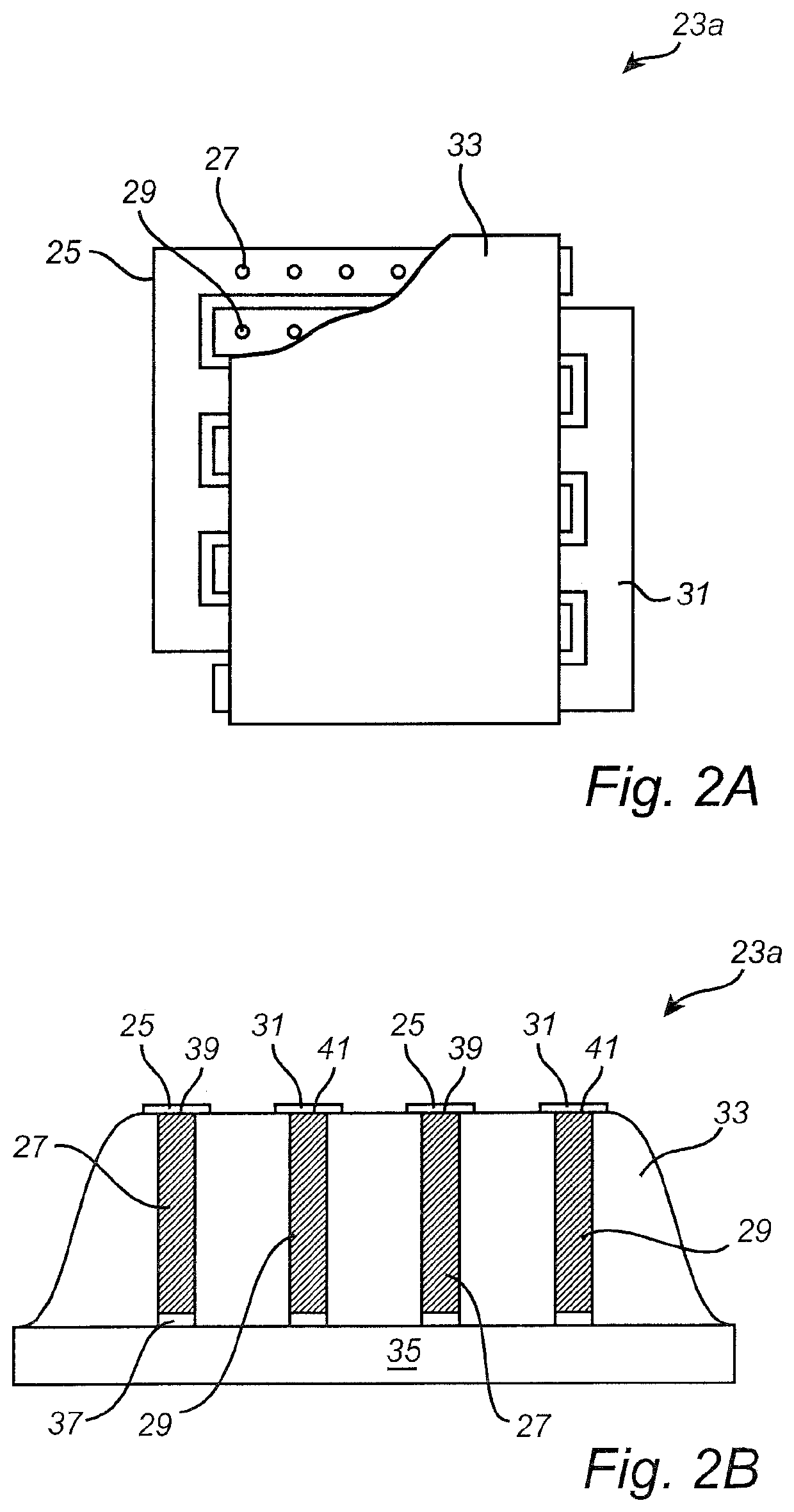
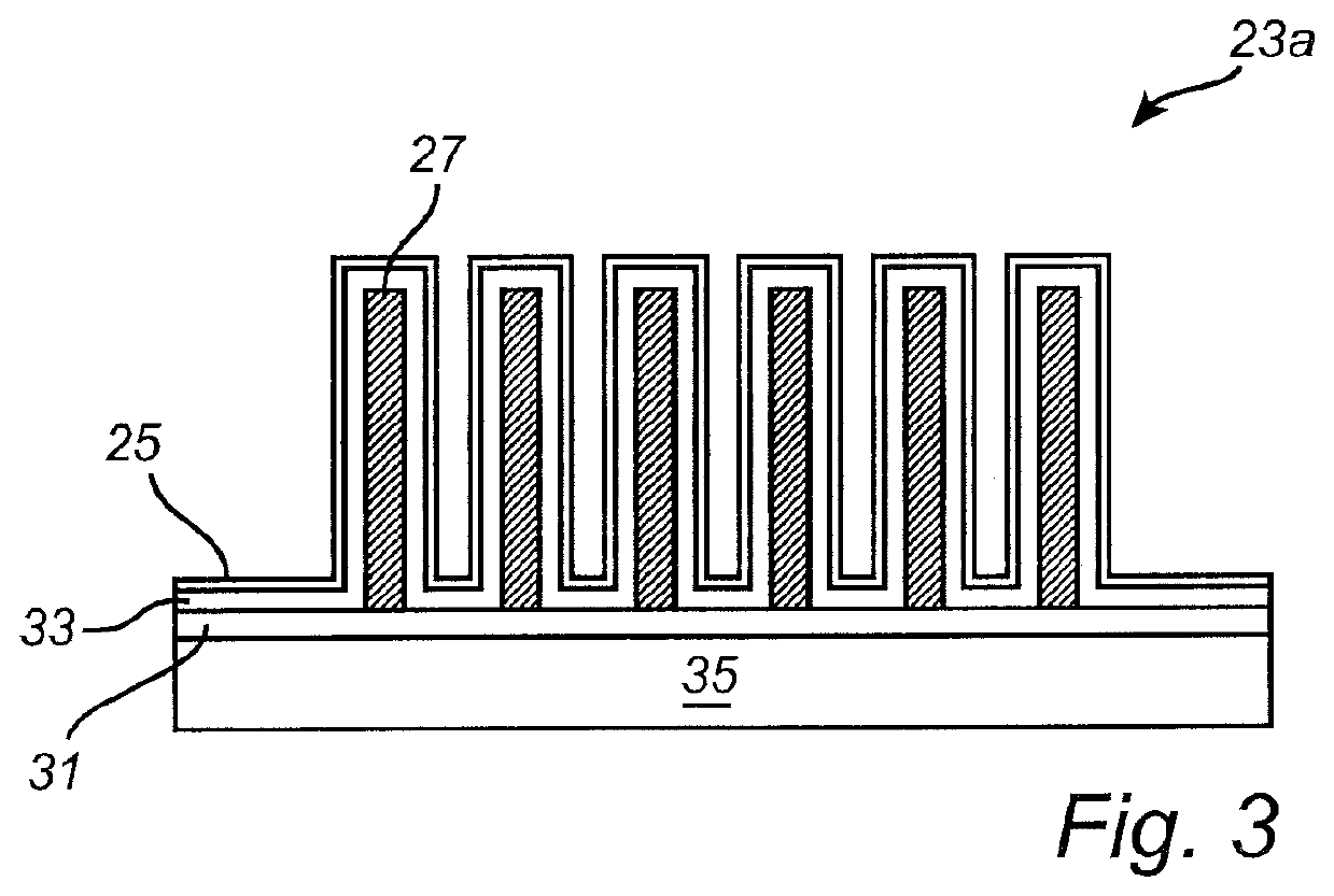
[0069]In the present detailed description, various embodiments of the energy storing interposer device is mainly described with reference to an energy storing interposer device comprising a nanostructure energy storage device in the form of a nanostructure capacitor.

[0070]It should be noted that this by no means limits the scope of the present invention, which equally well includes, for example, an interposer device comprising a nanostructure battery or a nanostructure capacitor and a nanostructure battery.

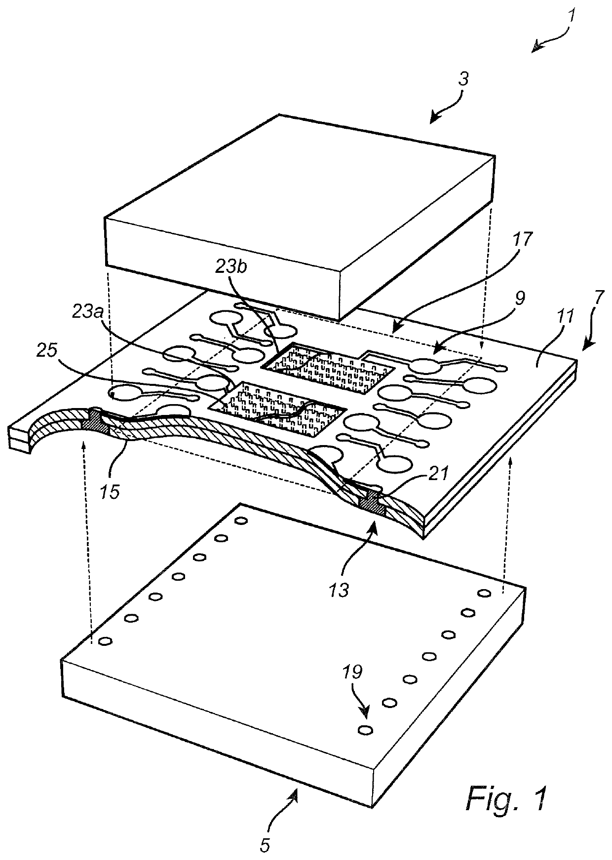
[0071]FIG. 1 schematically illustrates an electronic device 1 according to an embodiment of the present invention, comprising a first electrical circuit element, here in the form of a first integrated circuit (IC) 3, a second electrical circuit element, here in the form of a second IC 5, and an interposer device 7 according to an embodiment of the present invention, electrically and mechanically interconnecting the first IC 3 and the second IC 5.

[0072]The interposer device 7 compr...


PUM


Abstract

An interposer device comprising a first conductor pattern on a first side defining a portion of the interposer device to be covered by a first electrical circuit element; and a second conductor pattern on a second side to be connected to a second electrical circuit element. The second conductor pattern is electrically coupled to the first conductor pattern. The interposer device further comprises a plurality of nanostructure energy storage devices arranged within the portion of the interposer device to be covered by the first electrical circuit element. Each of the nanostructure energy storage devices comprises at least a first plurality of conductive nanostructures; a conduction controlling material embedding the nanostructures; a first electrode connected to each nanostructure in the first plurality of nanostructures; and a second electrode separated from each nanostructure in the first plurality of nanostructures by the conduction controlling material.

Description

FIELD OF THE INVENTION[0001]The present invention relates to an interposer device for electrically and mechanically interconnecting a first electrical circuit element and a second electrical circuit element. The present invention also relates to a method of manufacturing such an interposer device.BACKGROUND OF THE INVENTION[0002]Electronic devices need electrical energy to operate. In a portable electronic device, a battery is typically provided, and electrical energy is drawn from the battery to power integrated circuits comprised in the electronic device. Moreover, a number of driving factors that are continuously improving the system level performance including but not limited to smaller form-factor with higher data transfer rate, signal integrity, memory bandwidth, power and thermal management capability etc. It is of highest importance that the today's integrated and portable products are continuously striving to improve at least those metrics. The maturity of the Through Silic...

Claims


Application Information

Patent Timeline
IPC IPC(8): H01L23/522H01L23/00H01L23/29H01L21/768H01L49/02
CPCH01L28/40H01L24/05B82Y30/00H01L2224/02371H01L21/7684H01L23/5223H01L23/29H01L23/50H01L23/49822H01L24/97H01L23/498H01L23/528H01L23/525H01L23/485
Inventor KABIR, M. SHAFIQULJOHANSSON, ANDERSSALEEM, MUHAMMAD AMINANDERSSON, RICKARDDESMARIS, VINCENT
Owner SMOLTEK AB
Why Eureka
Try Eureka