

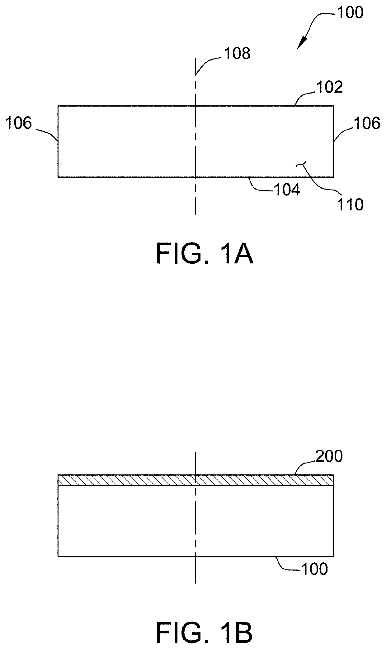
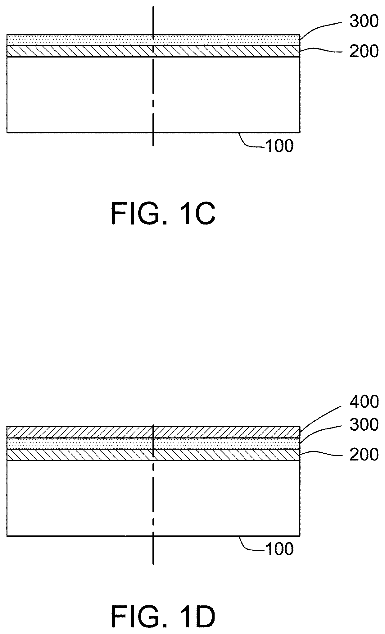
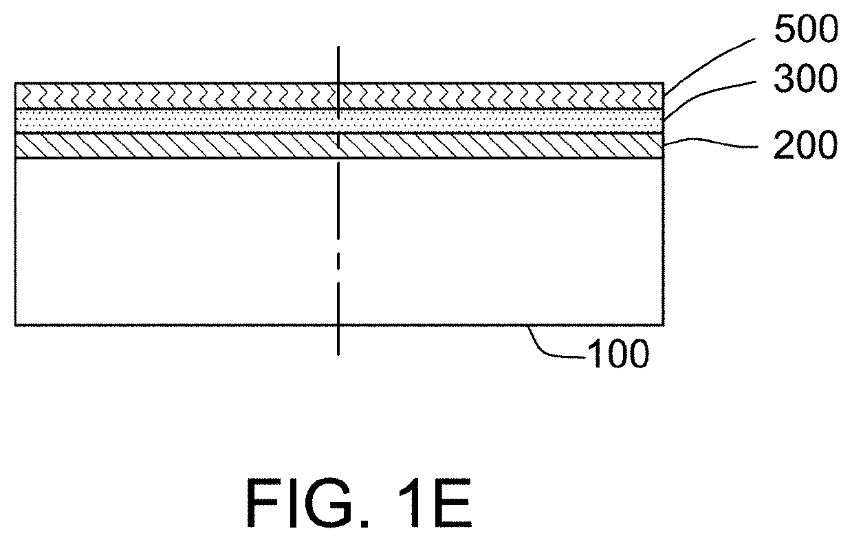
Direct formation of hexagonal boron nitride on silicon based dielectrics
a technology of hexagonal boron nitride and silicon based dielectrics, which is applied in the direction of semiconductor devices, electrical apparatus, transistors, etc., can solve the problems of poor electronic and thermal transport characteristics of silicon-based oxide and nitride substrates, rough and dopant-rich substrates,
- Summary
- Abstract
- Description
- Claims
- Application Information
AI Technical Summary
Benefits of technology
Problems solved by technology
Method used
Image

Examples
example 2
Synthesis by Chemical Vapor Deposition of Graphene on Cu Foil
[0085]High quality monolayer graphene was grown via chemical vapor deposition (CVD) process on a (1″×2″) copper foil (25 μm, 99.98% purity) using CH4 (99.95% purity, Praxair) as carbon feedstock, and H2 (99.9999%, Praxair) as reduction gas. A standard 1-inch quartz tube in a split CVD furnace (MTI OTF-1200X) was used as reaction chamber. The typical graphene synthesis was as follows. First, the copper foil was thoroughly washed with copious amount of water, acetone, and IPA (in the order). The native oxide of Cu foil was then removed by submerging in solution of Fe(NO3)2:HNO3 (1M:3M) for 10 minutes. Subsequently, the Cu foil was continuously rinsed with copious amount of water, acetone, and IPA (in the order). In order to further remove the remaining ion, the Cu foil was sonicated in 100 mL of acetone (ACS spectrophotometric grade, ≥99.5%, Fisher Scientific). Then the foil was thoroughly washed with copious amount water, a...
example 4
ect Transistor (FET) Device Fabrications and Electrical Measurements
[0087]Photolithography:
[0088]After transferring to highly n++ silicon substrates with different dielectric layers (SiN, and hBN / SiN), the graphene samples were deposited with Cr / Au (15 nm / 95 nm) layers. A positive photoresist (AZ 1818) was spin-coated onto the samples at 4000 rpm for 45 second. The samples were then baked on the hot plate at 110° C. for 1 minute. Subsequently, a dose of UV light (365 nm and lamp power of 900 W) was introduced into the samples with aligned mask for 12 second using Karl Suss MA6 mask aligner. Then samples were developed in a solution of 3:1 (DI water: AZ 340) for 18 seconds followed by etching the un-protected Cr / Au area to form the electrode contact in Au etchant (36 seconds), and Cr etchant (18 seconds) at room temperature in the order. After defining the metal contact, the samples were washed with copious amount of acetone and IPA (in the order), and dried with purified air flow fo...
PUM
| Property | Measurement | Unit |
|---|---|---|
| optical transparency | aaaaa | aaaaa |
| area | aaaaa | aaaaa |
| diameter | aaaaa | aaaaa |
Abstract
Description
Claims
Application Information