Semiconductor photocatalyst and preparation method thereof

a technology of photocatalyst and semiconductor, applied in the field of semiconductor photocatalyst and preparation method thereof, can solve the problems of high risk and danger of these pollutants, destroying the microbial population in soil and water, and reducing the immunity of microorganisms and bacteria, so as to reduce the generation of reactive oxygen species, reduce the process efficiency, and reduce the effect of efficiency

Active Publication Date: 2020-05-21
PARAPARI MOHAMMAD HAGHIGHI +2
View PDF0 Cites 18 Cited by
  • Summary
  • Abstract
  • Description
  • Claims
  • Application Information

AI Technical Summary

Problems solved by technology

Currently, increasing organic pollutants such as pharmaceuticals, personal care products, insecticides and dyes in surface water and the environment have made these types of pollutants as one of the most important and serious challenges of the human society.
It is worth noting that the risks and dangers of these pollutants are high even at low concentrations.
Among the pharmaceuticals used, antibiotics, in addition to being resistant, high persistence and creating toxicity in the environment, can destroy the microbial population in the soil and water and also cause the immunity of microorganisms and bacteria.
Hence, antibiotic-contaminated water and soil have increasingly become a problem in society.
Nevertheless, the design of a nanophotocatalyst with high activity in the sunlight spectrum, facilitating intra-particle mass transfer, increasing surface adsorption phenomenon, improving surface reactions, facilitating the separation of photocatalyst from treated aqueous solution and high physico-chemical stability still is one of the main challenges of photocatalytic process.
Because despite their high / suitable activity, the use of them have limited due to the wide band gap, high rate of charge carrier recombination, low surface adsorption, the separation problem and etc.

Method used


Image

  • Semiconductor photocatalyst and preparation method thereof
  • Semiconductor photocatalyst and preparation method thereof
  • Semiconductor photocatalyst and preparation method thereof

Examples


example 1

sis

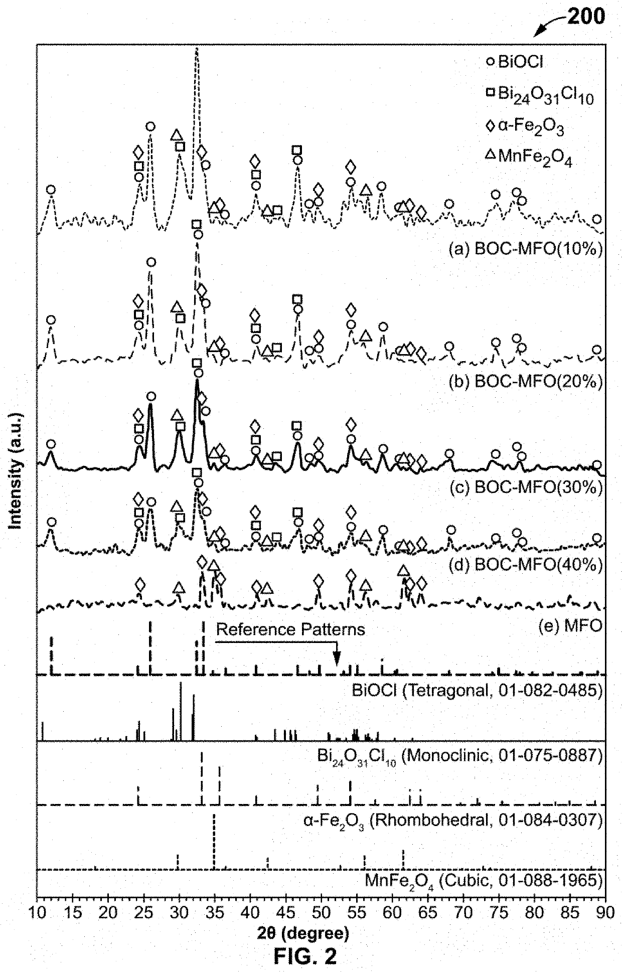
[0067]Referring to FIG. 2, exemplarily illustrates a graph 200 of X-ray diffraction patterns of BiOCl—Bi24O31Cl10 / MnFe2O4—Fe2O3 semiconductor is disclosed. Results relevant to the X-ray powder diffraction (XRD) analysis of BOC-MFO of 10 wt %, BOC-MFO of 20 wt %, BOC-MFO of 30 wt % and BOC-MFO of 40 wt % and MFO are illustrated in FIG. 2. For BOC-MFO nanocomposites with various amounts of MFO, the characteristic peaks were well indexed to the phase of BiOCl with the tetragonal crystal structure and the lattice parameters a=b=3.887 and c=7.354 Å (JCPDS NO. 01-082-0485), the monoclinic Bi24O31Cl10 with the lattice constants a=9.995, b=3.969 and c=9.440 Å (JCPDS NO. 01-075-0887), the α-Fe2O3 phase with the rhombohedral crystal structure (JCPDS File: 01-084-0307) at 20=24.2, 33.2, 35.7, 41.0, 49.6, 54.2, 62.6 and 64.2° and the cubic phase of MnFe2O4 (JCPDS File: 01-088-1965) at around 20=29.7, 35.0, 42.5, 56.2 and 61.7 that indicated in all nanocomposites synthesized by sono-solvother...

example 2

lysis

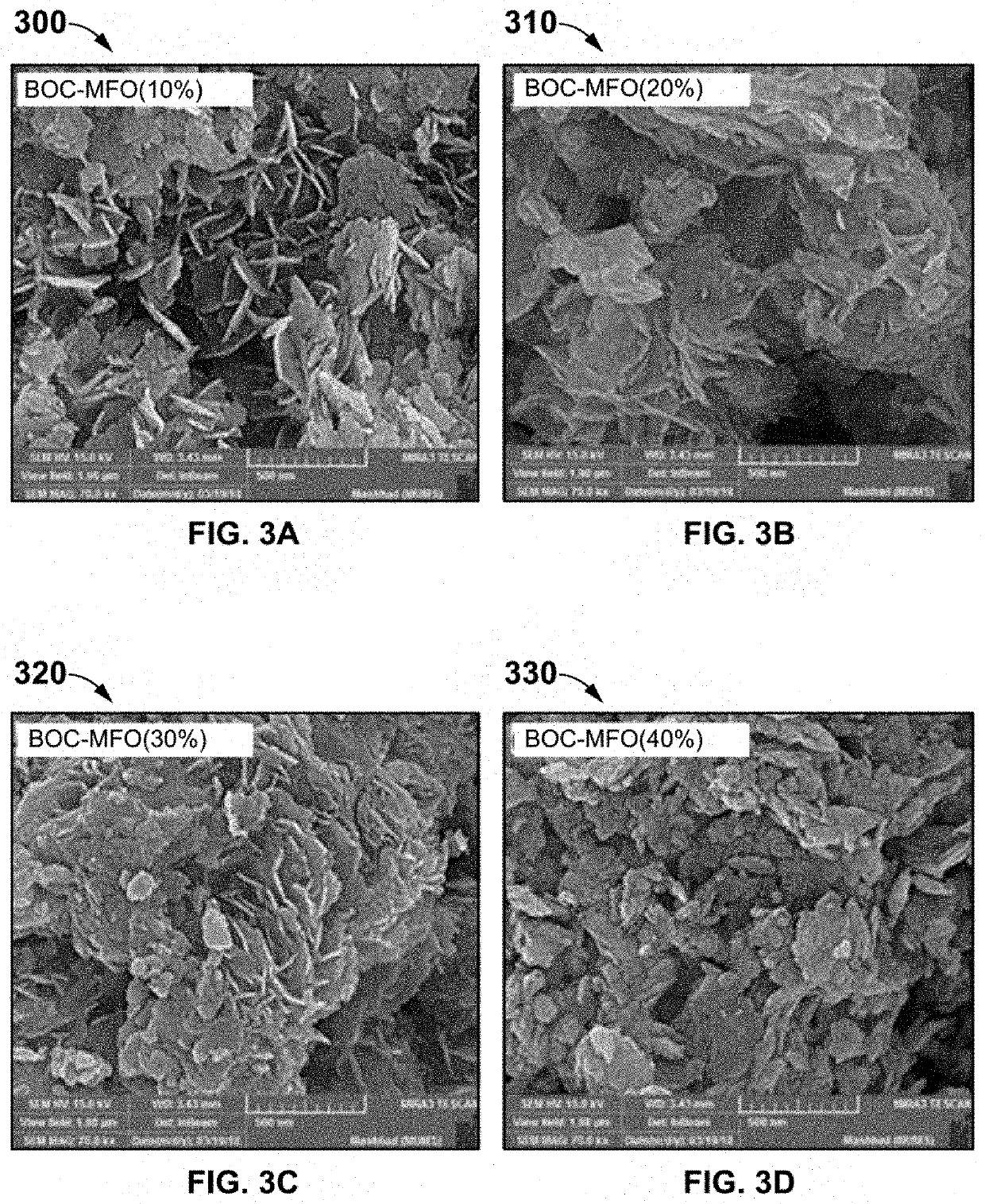
[0069]FESEM (field emission scanning electron microscopy) images (300, 310, 320, 330) of BOC-MFO of 10 wt %, BOC-MFO of 20 wt %, BOC-MFO of 30 wt % and BOC-MFO of 40 wt % samples are displayed in FIG. 3A-FIG. 3D, respectively. As observed, the magnetic BOC-MFO nano-photocatalyst of 10 wt % has the nanosheet morphology, which these nanosheets contain nanoparticles of MFO. With increasing the content of MFO, the existing nanosheets were gradually stacked together, leading to the formation of plate-like clusters. The reason of the stacking and agglomeration of nanosheets and particles could be attributed to the interaction between magnetic nanoparticles. So that, with increasing the content of MFO, the stacking and agglomeration phenomenon was increased. This event could lead to a decrease in the surface adsorption and consequently a decrease in the photocatalytic activity of sample.

[0070]Referring to FIG. 4A-FIG. 4D, the surface structure of the BOC-MFO nano-photocatalyst of 10 w...

example 3

apping Analysis

[0071]Referring to FIG. 5A, the presence of Bi, O, Cl, Mn and Fe elements is confirmed in the structure of BOC-MOF (10%) sample from the EDX (energy dispersive X-ray) analysis image 500. A dot-mapping image 510 of all elements is represented in FIG. 5B.

[0072]FIG. 5C exemplarily illustrates a dot-mapping image 520 of Bi in BiOCl—Bi24O31Cl10 / MnFe2O4—Fe2O3 semiconductor of 10 wt %, according to an embodiment of the present invention. FIG. 5D exemplarily illustrates a dot-mapping image 530 of Cl in BiOCl—Bi24O31Cl10 / MnFe2O4—Fe2O3 semiconductor of 10 wt %, according to an embodiment of the present invention.

[0073]FIG. 5E exemplarily illustrates a dot-mapping image 540 of Mn in BiOCl—Bi24O31Cl10 / MnFe2O4—Fe2O3 semiconductor of 10 wt %, according to an embodiment of the present invention. FIG. 5F exemplarily illustrates a dot-mapping image 550 of Fe in BiOCl—Bi24O31Cl10 / MnFe2O4—Fe2O3 semiconductor of 10 wt %, according to an embodiment of the present invention. Moreover, the ...


PUM

PropertyMeasurementUnit
frequencyaaaaaaaaaa
temperatureaaaaaaaaaa
size distributionaaaaaaaaaa

Abstract

The present invention discloses a novel magnetic BiOCl—Bi24O31Cl10 / MnFe2O4—Fe2O3 semiconductor photocatalyst as a staggered multi-heterojunction nano-photocatalyst for pharmaceutical effluents remediation, and preparation method and use thereof. The semiconductor photocatalysts are at weighted ratios 9:1 4:1, 7:3 and 3:2 of BiOCl—Bi24O31Cl10 and MnFe2O4—Fe2O3 semiconductor. The BiOCl—Bi24O31Cl10 / MnFe2O4—Fe2O3 semiconductor photocatalyst with 10% MnFe2O4—Fe2O3 is a solar light activated photocatalyst for pharmaceutical effluents remediation. The pharmaceutical effluents include ofloxacin antibiotic. The mentioned semiconductor photocatalyst effectively removes the ofloxacin (OFL) antibiotic from polluted aqueous solution under simulated solar light, facilitates separation of photocatalyst from treated aqueous solution using magnetic property, enhances light absorption edge, improves intra-particle mass transfer, increases adsorption capacity and promotes efficient surface reactions, which includes: increasing the light absorption range, increasing quantum efficiency and reducing the recombination phenomenon.

Description

BACKGROUND OF THE INVENTION[0001]Currently, increasing organic pollutants such as pharmaceuticals, personal care products, insecticides and dyes in surface water and the environment have made these types of pollutants as one of the most important and serious challenges of the human society. Amongst the organic matter, pharmaceuticals are highly consumed by both humans and livestock in veterinary treatment. These do not significantly metabolize and are excreted from the body as unchanged or in the form of metabolic products through the urine and discharged into municipal sewage and subsequently entered into the environment.[0002]The most common pharmaceuticals found in the environment are antibiotics, analgesic drugs, chemotherapy drugs and hormones. Worldwide, a wide range of these drugs (as emerging contaminants (ECs)) have been observed in the soil and aquatic environments, indicating their resistance in contrast to commonly used technologies in the wastewater treatment. It is wor...

Claims


Application Information

Patent Timeline
Patent Type & Authority Applications(United States)
IPC IPC(8): B01J35/00B01J37/34B01J35/10B01J37/08B01J37/06B01J37/00B01J23/889
CPCB01J35/1047B01J23/8892B01J37/343B01J35/1019B01J37/06B01J37/08B01J35/1042B01J37/009B01J35/004B01J35/108B01J27/128B01J35/0006B01J35/002B01J35/0033B01J35/1061B01J37/031
Inventor PARAPARI, MOHAMMAD HAGHIGHIMOLLASARAEI, MARYAM SHABANIPARAPARI, AMIR HAGHIGHI
Owner PARAPARI MOHAMMAD HAGHIGHI
Why Eureka
Try Eureka