CMOS RF power limiter and ESD protection circuits

a technology of power limiters and protection circuits, applied in the field of radio frequency (rf) power limiters and electrostatic discharge (esd) circuitry, can solve the problems of affecting the reliability of power amplifiers. the last stage of the transmit chain is subject to the highest voltage stress, so as to reduce the risk of voltage and current over-stress, reduce the effect of power over-stress

Active Publication Date: 2020-06-04
OCTOTECH INC +1
View PDF0 Cites 5 Cited by
  • Summary
  • Abstract
  • Description
  • Claims
  • Application Information

AI Technical Summary

Benefits of technology

[0010]An additional objective of the present invention is to provide for mitigation of voltage and current over-stress of transistors utilized in RF transceiver circuits. Generally, the circuit architectures allow input power levels to be limited to an extent that reliable operation can be maintained.
[0011]Additionally, the proposed solutions consume much smaller area compared to prior art solutions, they do not require a bias current or voltage be applied, and they do not require additional matching circuitry. Finally, the proposed solutions may be integrated into transceiver circuits that are fabricated in CMOS technology or applied as standalone devices.

Problems solved by technology

Conventional transceivers typically do not generate sufficient power or have sufficient sensitivity for reliable communications standing alone.
The long-term reliability of the power amplifier may be compromised at these input power levels to the power amplifier, as there may be excessive voltage stress on the transistors thereof.
The transistors in the last stages of the transmit chain are subject to the highest voltage stresses, as the previous stages amplify the input signal to levels high enough to cause damage.
This is particularly problematic in CMOS (complementary metal oxide semiconductor) transistors that have lower breakdown voltage ratings compared to conventional BiCMOS or GaAs (gallium arsenide) technologies.
The transistors in the last amplifier stage are subject to additional stresses beyond that which is associated with the large input signal alone when the output is not perfectly matched to the 50 Ohm load.
This may result in the voltage level at the transistor terminals far exceeding that for reliable operation.

Method used


Image

  • CMOS RF power limiter and ESD protection circuits
  • CMOS RF power limiter and ESD protection circuits
  • CMOS RF power limiter and ESD protection circuits

Examples


Embodiment Construction

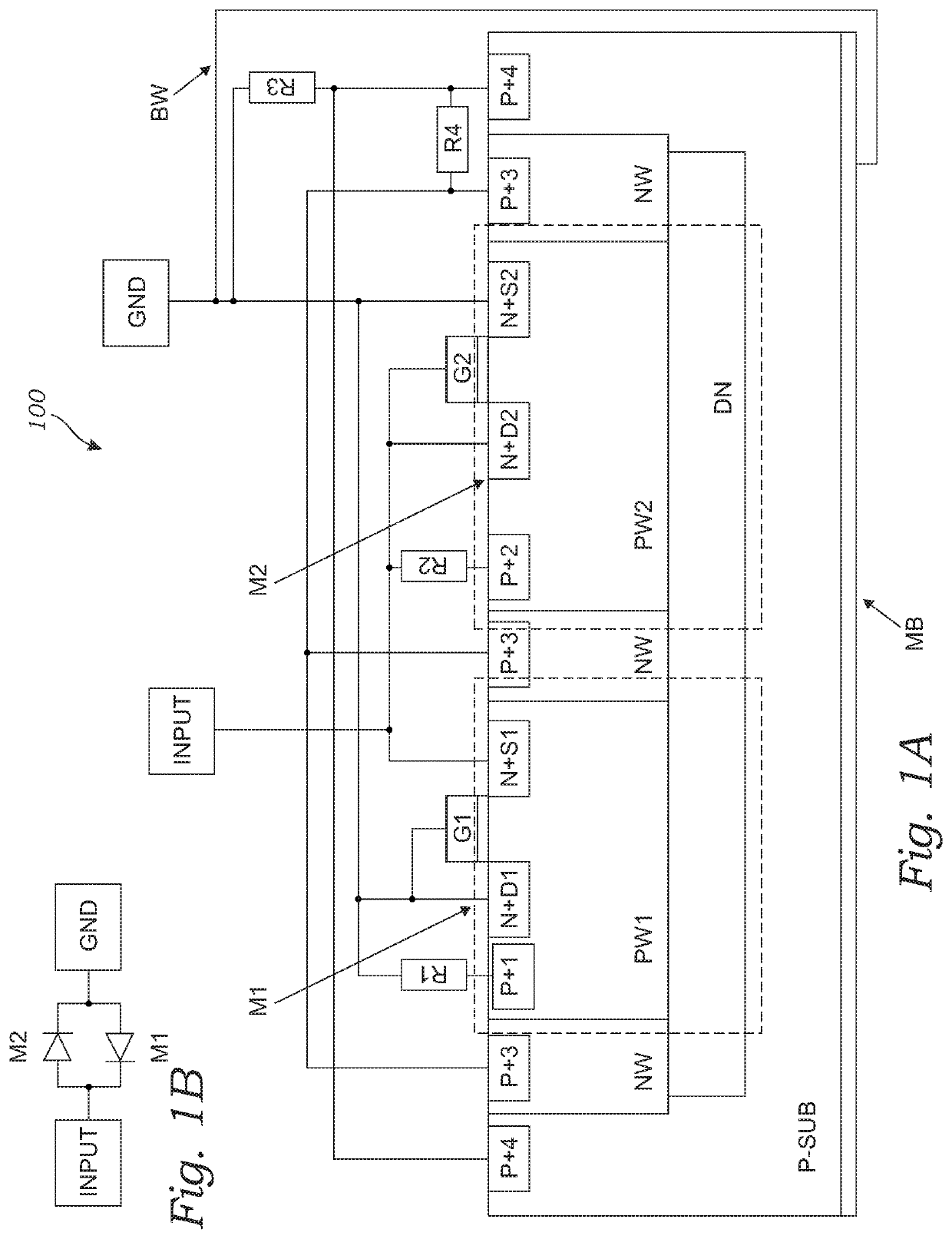
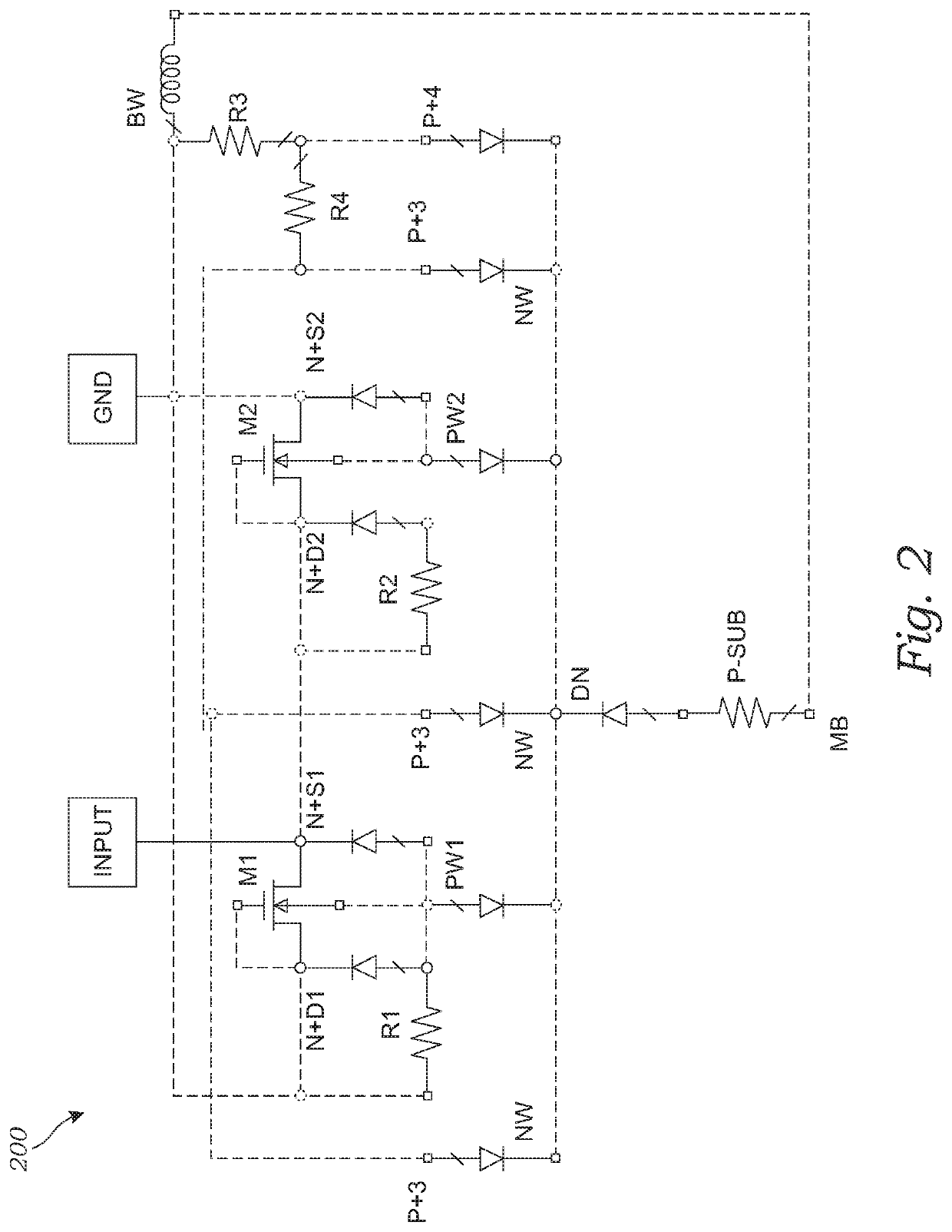
[0027]Various embodiments of a CMOS integrated circuit with RF power limiting and ESD protection capabilities are described herein. In the following description, numerous specific details are set forth in order to provide a thorough understanding of the present invention. One skilled in the relevant art will recognize, however, that the techniques described herein can be practiced without one or more of the specific details, or with other methods, components, materials, etc. In other instances, well-known structures, materials, or operations are not shown or described in detail to avoid obscuring certain aspects. A substrate may have a front side and a back side. Any fabrication process that is performed from the front side may be referred to as a frontside process while any fabrication process that is performed from the back side may be referred to as a backside process. Structures and devices such as diodes, resistors and associated transistors may be formed in a front surface of ...


PUM


Abstract

An RF power limiter and ESD protection circuit has a set of two CMOS FETs each configured to perform a diode function with a defined forward voltage and arranged in an anti-parallel configuration and coupled between the input terminal and the ground terminal. When an RF signal is applied symmetrically to the input terminal and ground terminal it becomes symmetrically attenuated when the signal level exceeds the defined forward voltage of the diode configured CMOS FETs. In the ESD protection mode one of the CMOS FETs acts as a grounded gate NMOS transistor with SCR action to provide for mitigation of voltage and current over-stress of transistors utilized in RF transceiver circuits. Generally, the circuit architectures allow input power levels to be limited to an extent that reliable operation can be maintained.

Description

CROSS-REFERENCE TO RELATED APPLICATIONS[0001]This application for a utility patent claims the benefit of U.S. Provisional Application No. 62 / 772,989, filed Nov. 29, 2018.BACKGROUND OF THE INVENTIONField of the Invention[0002]This invention relates generally to radio frequency (RF) power limiting and electrostatic discharge (ESD) circuitry, and more particularly to transceiver architectures with input power protection circuits used, for example, in mobile communications systems.Description of Related Art[0003]Wireless communications systems find applications in numerous contexts involving information transfer over long and short distances alike, and there exists a wide range of modalities suited to meet the particular needs of each. Chief amongst these systems with respect to popularity and deployment is the mobile or cellular phone.[0004]A fundamental component of any wireless communications system is the transceiver, that is, the combined transmitter and receiver circuitry. The tra...

Claims


Application Information

Patent Timeline
Patent Type & Authority Applications(United States)
IPC IPC(8): H01L27/02H03F1/26H03F3/21H04B1/18H03G11/00
CPCH03F1/26H03F3/21H01L27/0288H04B1/18H03G11/006H01L27/0262H01L27/0274H03F1/52H03F3/195H03G11/02
Inventor GORBACHOV, OLEKSANDRZHANG, LISETTE L.MILKOVITS, STEPHEN
Owner OCTOTECH INC
Why Eureka
Try Eureka