Single crystalline diamond part production method for stand alone single crystalline mechanical and optical component production
- Summary
- Abstract
- Description
- Claims
- Application Information
AI Technical Summary
Benefits of technology
Problems solved by technology
Method used
Image
Examples
Embodiment Construction
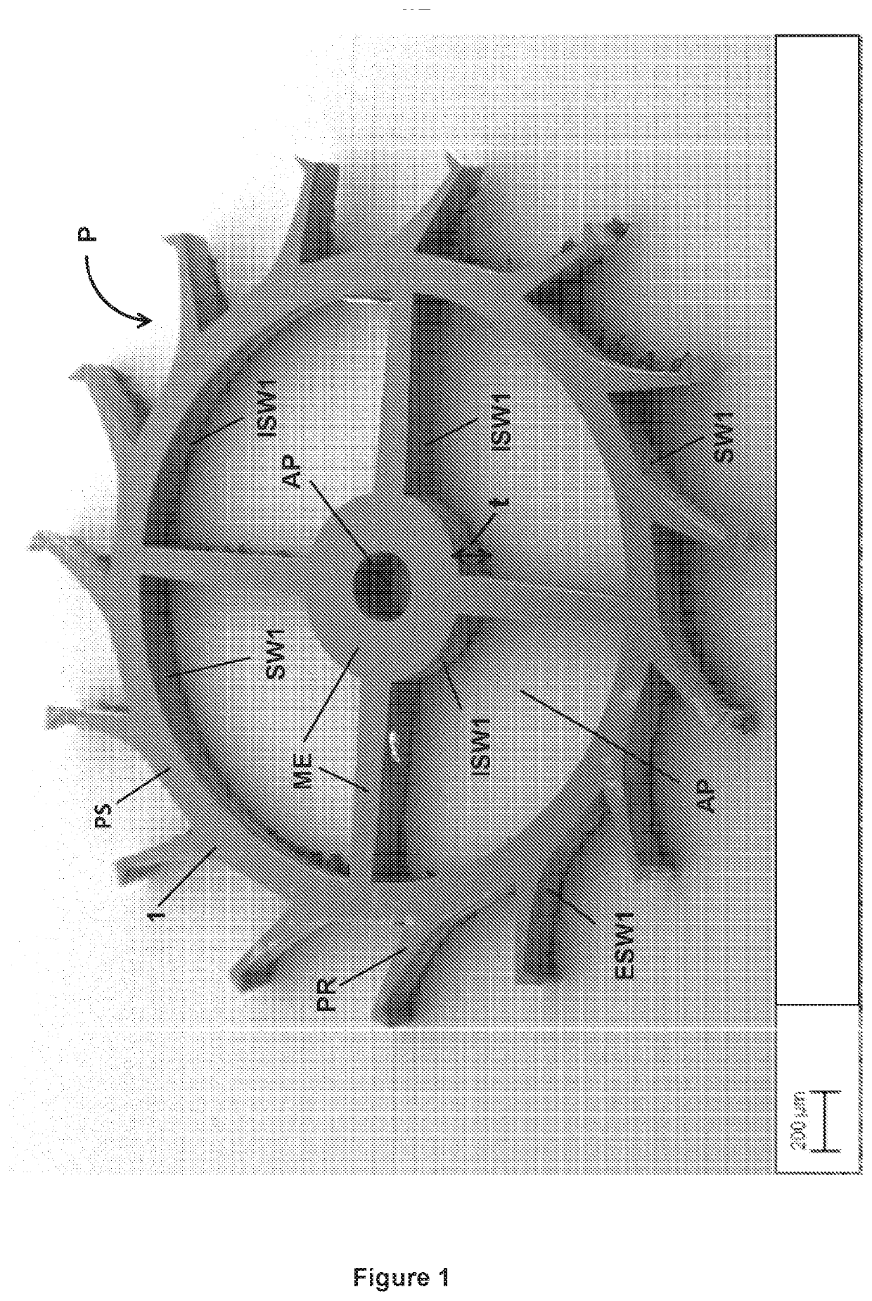
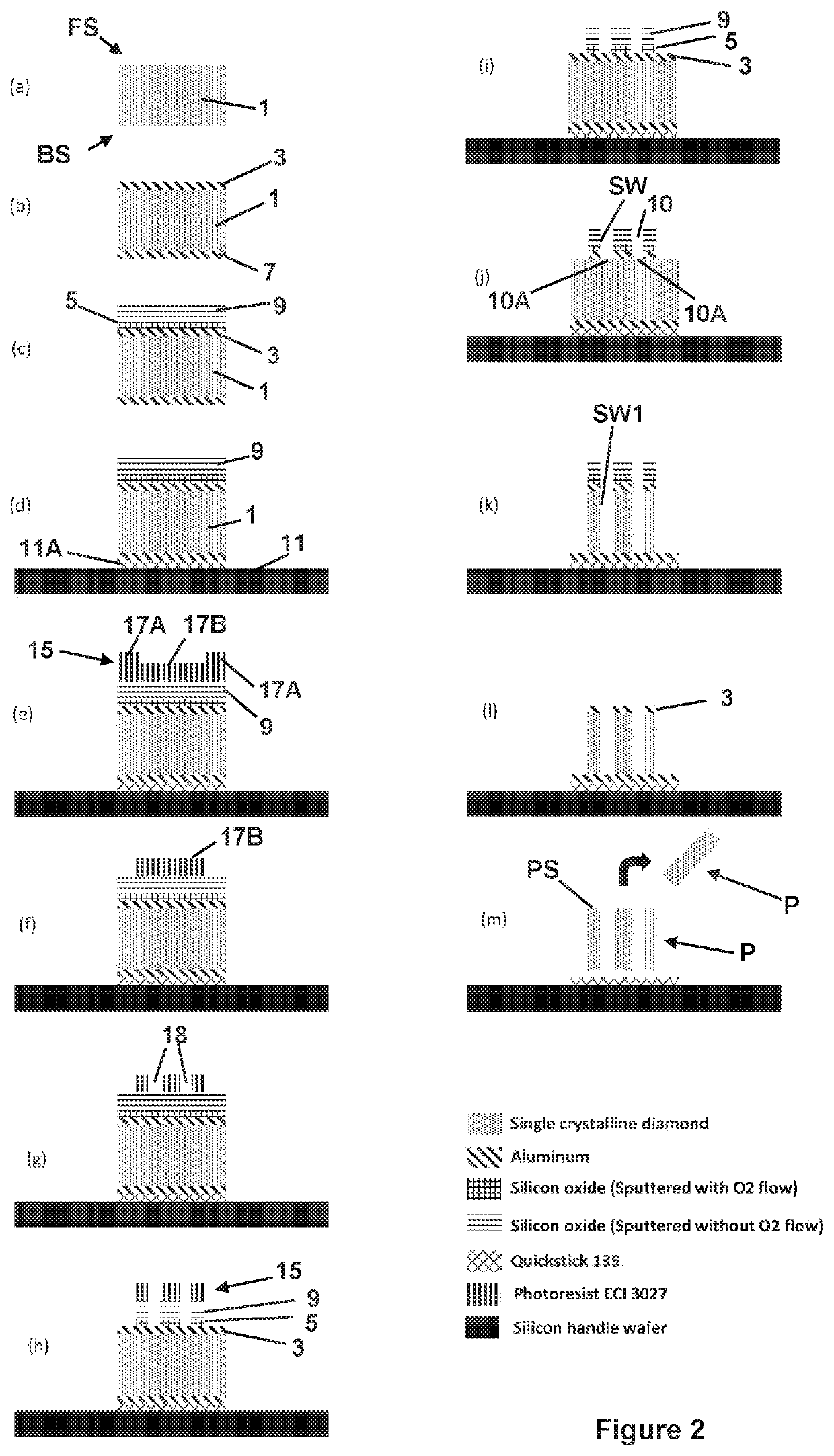
[0028]FIG. 2 shows an exemplary single crystalline diamond part fabrication method and FIG. 1 shows an exemplary diamond product P produced by this method. The method of the present disclosure is, for example, for fabricating micro-mechanical and micro-optical components or parts in single crystalline diamond.
[0029]The process uses single or mono crystal or crystalline diamond substrates or layers 1. The single crystalline diamond substrates or layers can, for example, be of dimensions 5 mm (length (x-direction)) x5 mm (width (y-direction)) x 0.15 mm (thickness t (z-direction)). However, the method of the present disclosure is not limited to such dimensions and the single crystalline diamond substrate or layer 1 can be larger or shorter in length and width and can also have a larger or smaller thickness. For example, diamond components of thicknesses between 1 μm and 1 mm can be produced and the single crystalline diamond substrate or layer 1 thus also has a thickness between 1 μm a...
PUM
| Property | Measurement | Unit |
|---|---|---|
| Thickness | aaaaa | aaaaa |
| Thickness | aaaaa | aaaaa |
| Adhesion strength | aaaaa | aaaaa |
Abstract
Description
Claims
Application Information

