Vapor phase epitaxial growth device

Active Publication Date: 2020-08-27
NAGOYA UNIVERSITY +1
View PDF0 Cites 0 Cited by
  • Summary
  • Abstract
  • Description
  • Claims
  • Application Information

AI Technical Summary

Benefits of technology

[0003]If long GaN crystal growth is enabled, a plurality of wafers can be produced from a single long crystal, by which substrate manufacturing cost can be reduced. However,

Problems solved by technology

Currently, a single wafer processing method which grows the GaN substrate

Method used


Image

  • Vapor phase epitaxial growth device
  • Vapor phase epitaxial growth device
  • Vapor phase epitaxial growth device

Examples


first embodiment

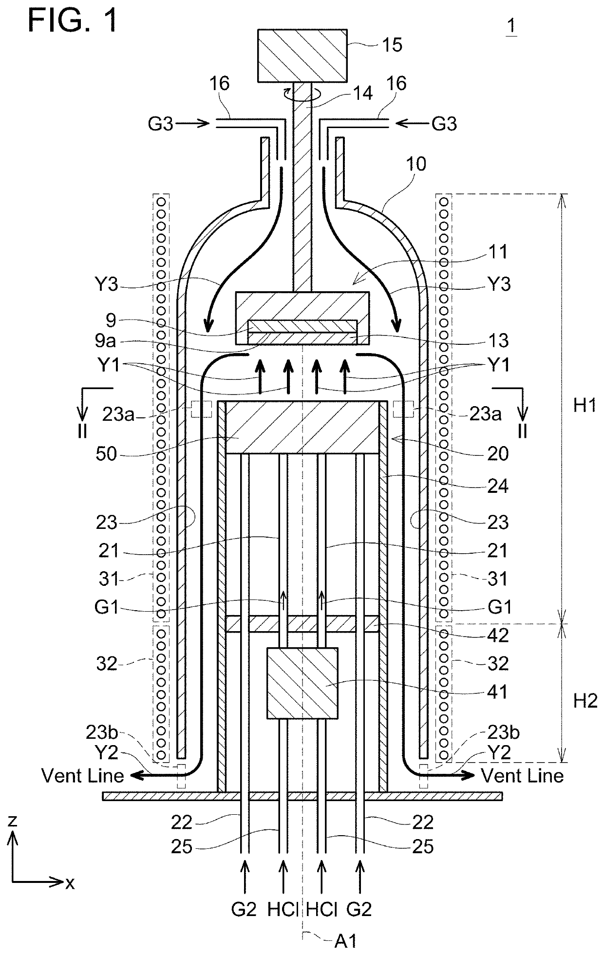
[0052]FIG. 1 shows a schematic cross-sectional view seeing a vapor phase epitaxial growth device 1 according to an aspect of the art disclosed herein along a lateral direction. The vapor phase epitaxial growth device 1 is an example of a device configuration for implementing a HVPE (Hydride / Halide Vapor Phase Epitaxy) method. The vapor phase epitaxial growth device 1 is provided with a reactor vessel 10. The reactor vessel 10 has a cylindrical shape. The reactor vessel 10 may be constituted of quartz. A material gas supply unit 20 and a wafer holder 11 are arranged within the reactor vessel 10.

[0053]A structure of the material gas supply unit 20 will be described. The material gas supply unit 20 is a cylindrical member. The material gas supply unit 20 is provided with a cylindrical cover 24. A disk-shaped shower head 50 is arranged at an upper end of the cover 24. Inlets of HCl gas supply pipes 25 and inlets of second material gas supply pipes 22 are arranged at a lower portion of t...

second embodiment

[0078]FIG. 5 shows a schematic cross-sectional view seeing a vapor phase epitaxial growth device 1a according to an aspect of the art disclosed herein along a lateral direction. Since members having same reference signs between the vapor phase epitaxial growth device 1a of FIG. 5 and the vapor phase epitaxial growth device 1 of FIG. 1 are identical, description thereof will be omitted.

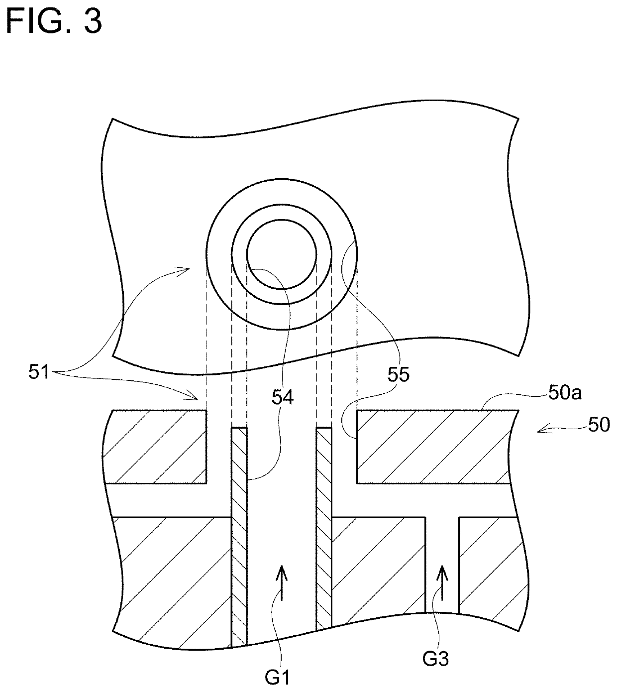
[0079]A first valve 61 is arranged at an inlet of each of HCl gas supply pipes 25. The first valves 61 are configured to control supplies of a gas containing HCl. A second valve 62 is arranged at an inlet of each of second material gas supply pipes 22. The second valves 62 are configured to control supplies of a gas containing a second material gas G2. A partition wall 42 functions as a heat insulator.

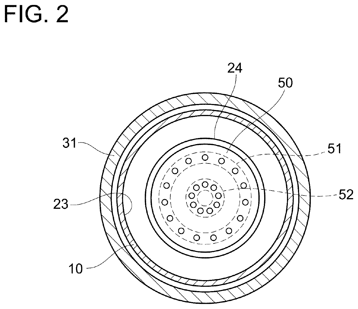
[0080]FIG. 2 is a view seeing a cross-section along a line II-II in FIG. 5 from vertically above. Regions on a surface of a shower head 50 where first nozzles 51 and second nozzles 52 are not provided are...

third embodiment

[0089]FIG. 6 is a schematic cross-sectional view seeing a vapor phase epitaxial growth device 201 according to a third embodiment along the lateral direction. The vapor phase epitaxial growth device 201 is an example of a device configuration for implementing the HVPE method. The vapor phase epitaxial growth device 201 is provided with a reactor vessel 210, a susceptor 216, a first material gas supply pipe 221, a second material gas supply pipe 222, and a gas exhaust pipe 271. The susceptor 216 is accommodated within the reactor vessel 210. A wafer 213 is held on a wafer holding surface of the susceptor 216.

[0090]The reactor vessel 210 has the first material gas supply pipe 221 configured to supply a first material gas G1 and the second material gas supply pipe 222 configured to supply a second material gas G2 connected thereto. An inner diameter D11 of the second material gas supply pipe 222 is larger than an outer diameter D12 of the first material gas supply pipe 221. The first m...


PUM

PropertyMeasurementUnit
Temperatureaaaaaaaaaa
Lengthaaaaaaaaaa
Distanceaaaaaaaaaa

Abstract

A vapor phase epitaxial growth device comprises a reactor vessel and a wafer holder arranged within the reactor vessel. The wafer holder includes a wafer holding surface configured to hold a wafer with a wafer surface oriented substantially vertically downward. The device comprises a first material gas supply pipe configured to supply a first material gas and arranged below the wafer holding surface. The device comprises a second material gas supply pipe configured to supply a second material gas and arranged below the wafer holding surface. The device comprises a gas exhaust pipe configured to exhaust gases and arranged below the wafer holding surface. A distance between the gas exhaust pipe and an axis line passing through a center of the wafer holding surface is greater than distances between the axis line and each of the first material gas supply pipe and the second material gas supply pipe.

Description

[0001]The present application is a national stage filing under 35 U.S.C. § 371 of PCT / JP2018 / 033324, filed on Sep. 7, 2018 which claims priorities to Japanese Patent Application No. 2017-183987 filed on Sep. 25, 2017, Japanese Patent Application No. 2018-92435 filed on May 11, 2018, and Japanese Patent Application No. 2018-92438 filed on May 11, 2018, the contents of which are hereby incorporated by reference into the present application. The description herein discloses an art related to a vapor phase epitaxial growth device of a compound semiconductor.TECHNICAL FIELDBackground Art[0002]Establishment of a low-cost manufacturing method of a GaN substrate is in demand. Currently, a single wafer processing method which grows the GaN substrate on one-by-one basis is dominant, and this has been a cause of high cost. A relevant technique is described in JP 2002-316892 A.DISCLOSURE OF INVENTIONTechnical Problem[0003]If long GaN crystal growth is enabled, a plurality of wafers can be produ...

Claims


Application Information

Patent Timeline
IPC IPC(8): C30B35/00C30B29/38C30B29/36C30B29/16H01L21/205
CPCC30B29/38C30B29/36H01L21/205C30B35/007C30B29/16H01L21/31C23C16/455C30B25/14H01L21/0262H01L21/0254C30B29/406C23C16/4412Y10T117/00H01L21/02518C30B23/02C30B23/06
Inventor NITTA, SHUGOHONDA, YOSHIONAGAMATSU, KENTAROAMANO, HIROSHIFUJIMOTO, NAOKI
Owner NAGOYA UNIVERSITY
Why Eureka
Try Eureka