Surface defect measuring apparatus and method by microscopic scattering polarization imaging

a surface defect and imaging technology, applied in the field of surface defect detection methods and apparatuses, can solve the problems of energy loss, direct threat to the safety of the whole system, local cracking of elements, etc., and achieve the effects of improving scanning measurement speed, rapid detection of surface defects, and simplified system structur

Active Publication Date: 2021-01-14
SHANGHAI INST OF OPTICS & FINE MECHANICS CHINESE ACAD OF SCI
View PDF0 Cites 6 Cited by
  • Summary
  • Abstract
  • Description
  • Claims
  • Application Information

AI Technical Summary

Benefits of technology

[0035](3) In the present invention, the micro-polarizer array is adopted to acquire a single image by a camera, so that the intensity values of four polarization directions of 0°, 45°, 90° and 135° can be obtained simultaneously; a polarizer and a rotary mach

Problems solved by technology

The metal ions and contaminants from the residual polishing solution in scratches and pits strongly absorb the incident light causing that the elements are locally cracked and the safe operation of the whole system is directly threatened.
In addition, scattering of the incident light by surface defects can cause energy loss of imaging beams in an imaging system, the stray light becomes noise, the signal-to-noise ratio of the system is further reduced, and target signals cannot be extracted and analyzed.
In the field of semiconductor industry, defects such as open bubbles and scratches are key factors influencing the yield of wafers and cause very serious influence on the performance of the chips, even leading to the chips to be directly scrapped, thus, they are regarded as “wafer killers”.
Among them, the photothermal microscopic imaging technique (see Bertussi, B., et al., “High-resolution photothermal microscope: a sensitive tool for the detection of isolated absorbing defects in optical coatings,” Applied Optics, 2006, 45(7): 1410-1415) is based on t

Method used


Image

  • Surface defect measuring apparatus and method by microscopic scattering polarization imaging
  • Surface defect measuring apparatus and method by microscopic scattering polarization imaging

Examples


Embodiment Construction

[0039]The present invention is described in further detail below with reference to specific drawings and embodiment, which are not taken as limiting the scope of the present invention.

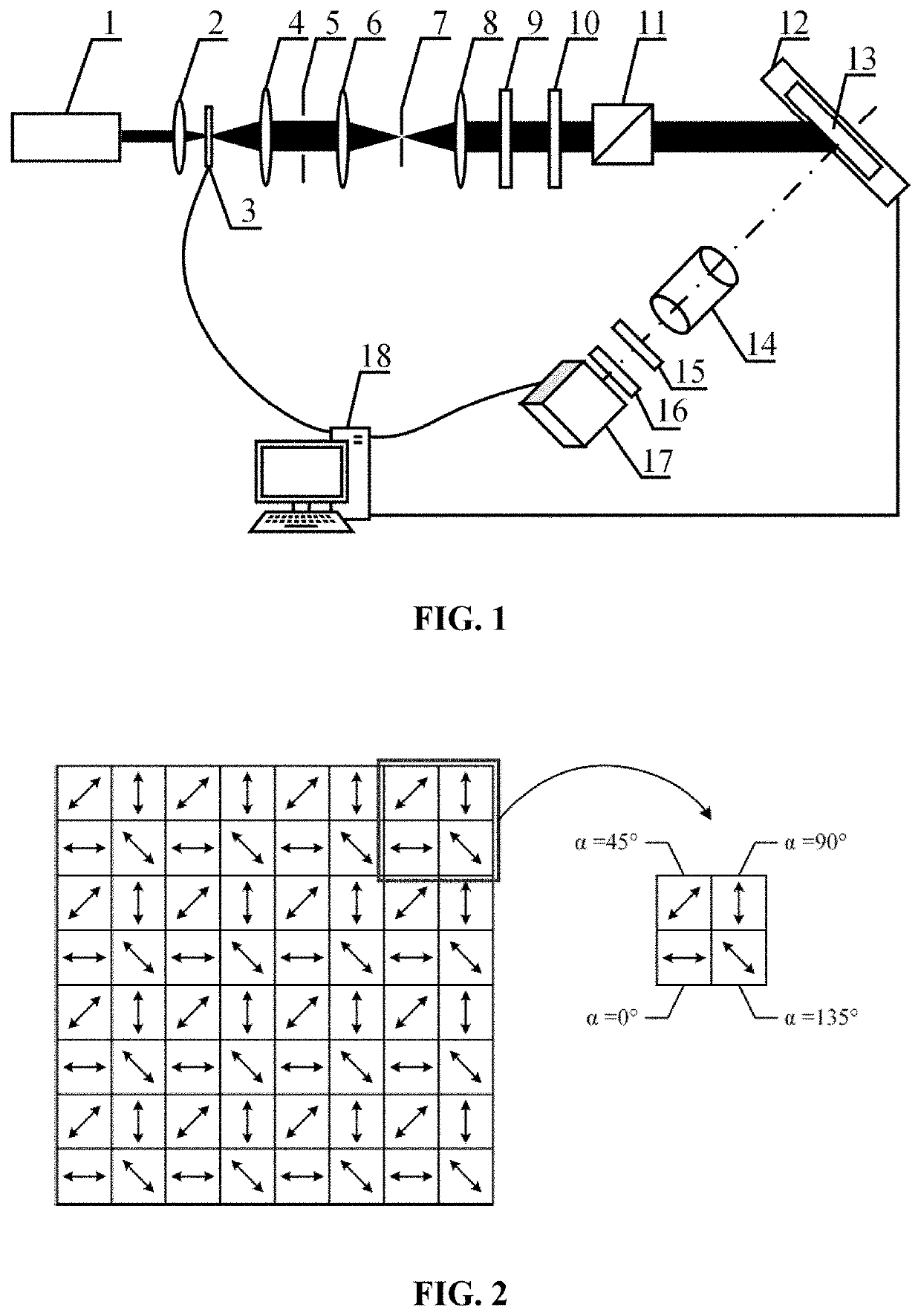
[0040]In one embodiment of the present invention as shown in FIG. 1, the surface defect measuring apparatus by the microscopic scattering polarization imaging in the present invention comprises a laser 1, a first converging lens 2, a rotary diffuser 3, a second converging lens 4, a diaphragm 5, a third converging lens 6, a pinhole 7, a fourth converging lens 8, a polarizer 9, a half-wave plate 10, a polarizing beam splitter 11, an X-Y translation stage 12, a sample 13, a microscope lens 14, a quarter-wave plate 15, a micro-polarizer array 16, a camera 17 and a computer 18.

[0041]The laser 1, the first converging lens 2, the rotary diffuser 3, the second converging lens 4, the diaphragm 5, the third converging lens 6, the pinhole 7, the fourth converging lens 8, the polarizer 9, the half-wave plate 10, a...


PUM


Abstract

A surface defect measuring apparatus and method by microscopic scattering polarization imaging is provided. The apparatus mainly comprises a laser, a first converging lens, a rotary diffuser, a second converging lens, a diaphragm, a third converging lens, a pinhole, a fourth converging lens, a polarizer, a half-wave plate, a polarizing beam splitter, an X-Y translation stage, a sample, a microscope lens, a quarter-wave plate, a micro-polarizer array, a camera and a computer. The micro-polarizer array is adopted to realize real-time microscopic scattering polarization imaging of the surface defects; a polarization-degree image is calculated to improve the sensitivity for detecting the surface defects of the ultra-smooth element, and the effective detection of the surface defects of a high-reflective coating element is also realized, and the requirement for rapid detection of the surface defects of a meter-scale large-aperture ultra-smooth element can be met.

Description

CROSS-REFERENCE TO RELATED APPLICATIONS[0001]The subject application is a continuation of PCT / CN2019 / 101282 filed on Aug. 19, 2019, which claims priority on Chinese Application No. CN201910609670.6 filed on Jul. 8, 2019 in China. The contents and subject matter of the PCT international application and Chinese priority application are incorporated herein by reference.FIELD OF TECHNOLOGY[0002]The present invention relates to method and apparatus for detecting surface defect, in particular, surface defect measuring apparatus and method by microscopic scattering polarization imaging for the surface of an ultra-smooth element.BACKGROUND ART[0003]Large-aperture ultra-smooth elements (the root mean square value of the surface roughness is less than 1 nm) are widely used in high-end equipment such as photolithography systems, high-power laser systems, astronomical telescope systems, and ultra-large-scale integrated circuits. In the high-power laser systems, defects, such as scratches and pi...

Claims


Application Information

Patent Timeline
IPC IPC(8): G01N21/21G01N21/49G01N21/88G02B21/08G02B21/00
CPCG01N21/21G01N21/49G01N21/8806G02B21/082G01N2201/0683G02B21/0032G02B21/0068G01N2021/8848G01N2201/06113G02B21/0036G01N21/9501G01N2021/4792G02B5/3025
Inventor SHAO, JIANDALIU, SHIJIENI, KAIZAOWANG, SHENGHAOZHOU, YOUWANG, WEIWEIXU, TIANZHULU, QI
Owner SHANGHAI INST OF OPTICS & FINE MECHANICS CHINESE ACAD OF SCI
Why Eureka
Try Eureka