
Methods of manufacturing a graphene-based device

a graphene-based device and manufacturing method technology, applied in the direction of chemically reactive gases, crystal growth processes, instruments, etc., can solve the problems of large scale, bulky and expensive pid devices, and damage to public health, and achieve the effect of increasing mechanical strength, reducing production costs, and reducing production costs

Pending Publication Date: 2021-08-05
UNIV OF MANCHESTER
View PDF0 Cites 0 Cited by
  • Summary
  • Abstract
  • Description
  • Claims
  • Application Information

AI Technical Summary

Benefits of technology

The patent discusses a method for protecting a layer of graphene during fabrication of a device. A UV barrier layer is used to shield the graphene from UV radiation and is removed after fabrication without affecting the graphene. The use of a flexible and stable polymer called SU8 polymer is also mentioned. The substrate used can be silicon, silicon dioxide, sapphire, or a semiconductor material. The invention allows for a higher yield of successfully fabricated areas of suspended graphene and can be used to produce devices with a large array of suspended layers of graphene.

Problems solved by technology

VOCs are emitted from solids or liquids with high vapor pressure and are often combustible and toxic leading to damaging affects on public health.
PID devices are bulky and expensive to make, however.
That being said, there are challenges in producing graphene-based devices, particularly on a large scale.
As an example, the fabrication techniques often employed in the manufacture of electronic components may damage or otherwise render the graphene less (or not at all) functional.
This is particularly true of devices that utilize suspended graphene, not least because the graphene is necessarily unsupported by the substrate in certain places.
Additionally, when monolayer graphene is laid over any solid insulating surface, its electronic properties are severely affected due to surface interactions and surface contaminations, which eventually reduce the dynamic sensitivity and other advantageous properties associated with graphene.

Method used


Image

  • Methods of manufacturing a graphene-based device
  • Methods of manufacturing a graphene-based device
  • Methods of manufacturing a graphene-based device

Examples


Embodiment Construction

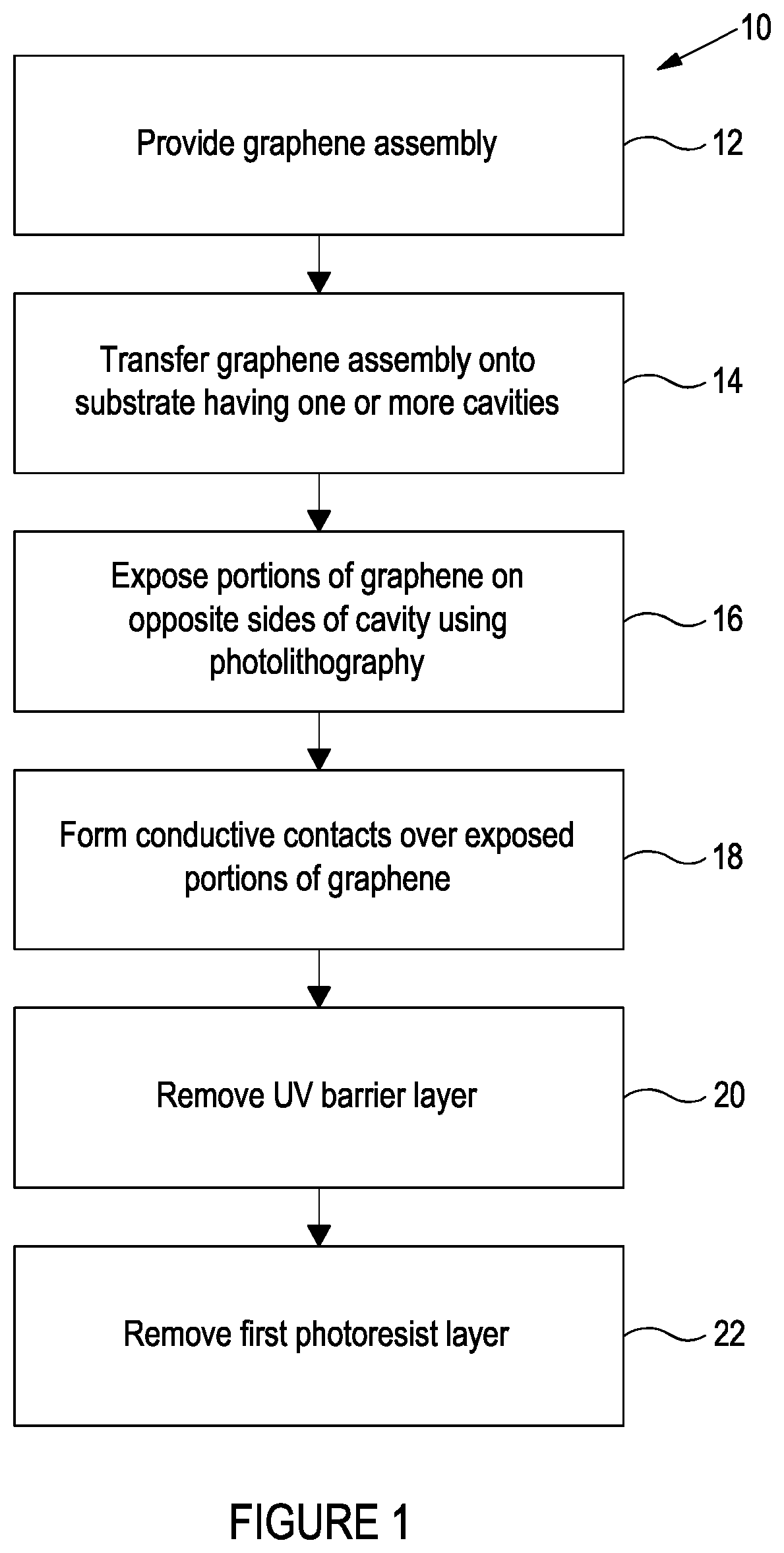
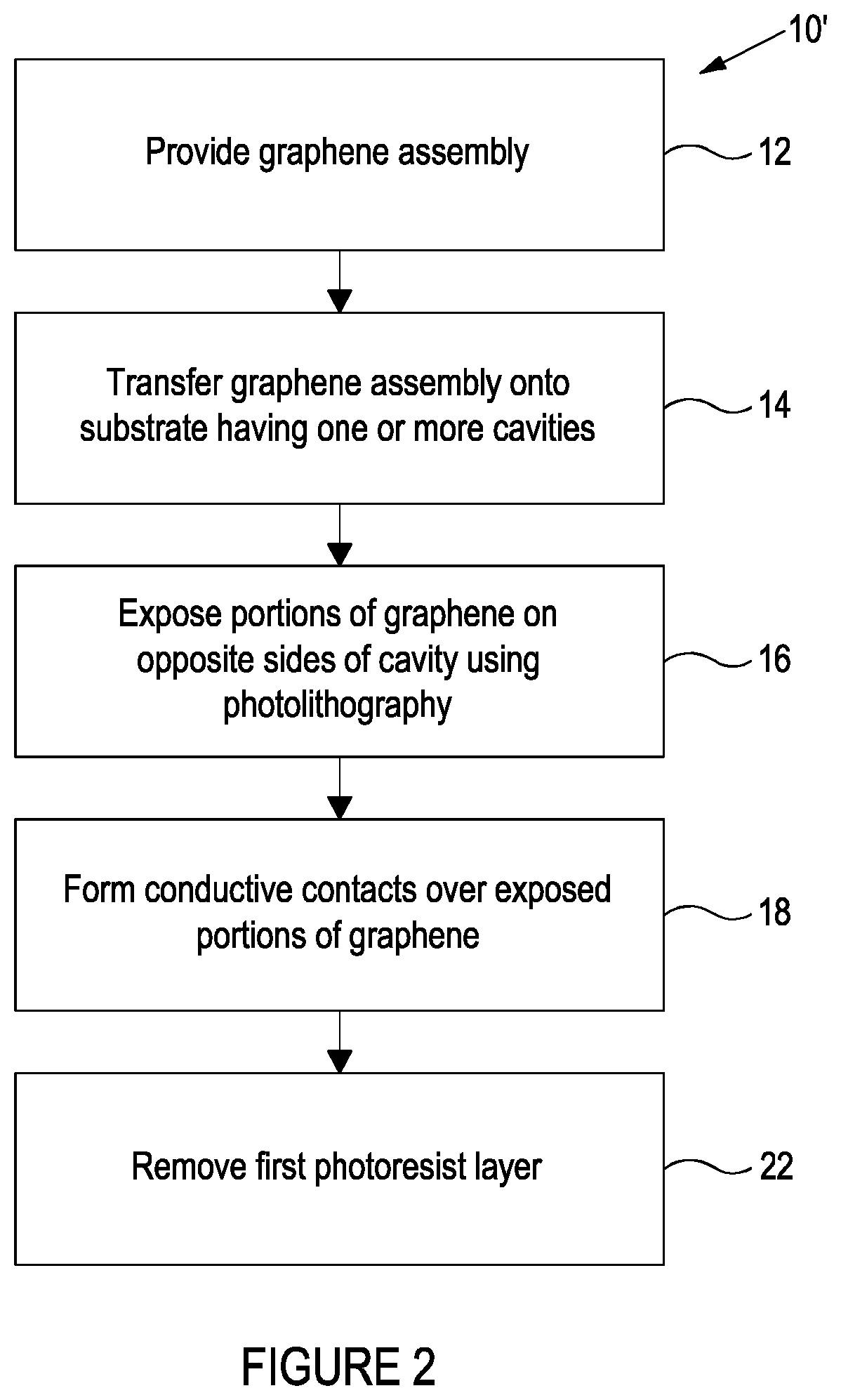
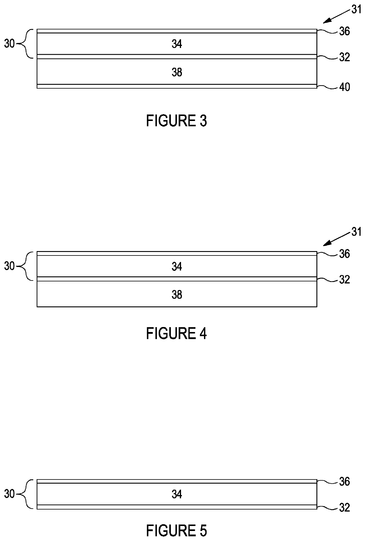
[0092]A method 10 of manufacturing a graphene-based device in accordance with an embodiment of the present invention is set out in FIG. 1. The method 10 comprises providing 12 a graphene assembly comprising one or more layers of graphene, a first photoresist layer disposed on the one or more layers of graphene, and an ultra-violet (UV) barrier layer disposed on the first photoresist layer on an opposite side to the one or more layers of graphene. The graphene assembly is transferred 14 onto a substrate comprising at least one cavity so that the one or more layers of graphene traverse the at least one cavity. Photolithography is used at step 16 to expose portions of the one or more layers of graphene on opposite sides of the at least one cavity and conductive contacts are formed at step 18 over the exposed portions of graphene. The UV barrier layer is then removed at step 20 and the first photoresist layer is removed at step 22.

[0093]A specific method of manufacturing a graphene-base...


PUM


Abstract

A method of manufacturing a graphene-baseddevice, comprising (i) providing a graphene assembly comprising one or more layers of graphene, a first photoresist layer disposed on the one or more layers of graphene, and an ultra-violet (UV) barrier layer disposed on the photoresist layer on an opposite side to the one or more layers of graphene; (ii) transferring the graphene assembly onto a substrate comprising at least one cavity so that the one or more layers of graphene traverse the at least one cavity; (iii) using photolithography to expose portions of the one or morelayers of graphene on opposite sides of the at least one cavity;(iv) forming conductive contacts over the exposed portions of graphene; (v) removing the UV barrier layer; and (vi) removing the first photoresist layer.

Description

[0001]This invention relates to methods of manufacturing a graphene-based device where, in particular, the graphene-based device includes one or more layers of graphene that each traverse a cavity formed in a substrate.BACKGROUND[0002]Graphene, a single atom thick 2D monolayer layer of carbon atoms, with its extraordinary physicochemical properties, high surface area (˜2630 m2g-1), thermal conductivity (˜5000 W / mK), electrical conductivity (mobility >15000 to 200,000 cm2V-1s-1) and mechanical strength (yield strength; ˜130 GPa, Young's modulus; 1 TPa) offers huge potential for use in sensor applications such as biosensors and chemical sensors. Since graphene does not have band gap, graphene needs to be modified (e.g. chemically or physically strained) to create a bandgap similar to that possessed by many semiconductor materials, and make the graphene suitable for use in electronic devices (such as switching devices, for example). Given that every atom in graphene is a surface ato...

Claims


Application Information

Patent Timeline
IPC IPC(8): H01L29/16H01L21/02C01B32/186
CPCH01L29/1606B82Y30/00C01B32/186H01L21/02527C30B25/22G01N27/4146H01L21/2007G01N27/125G01N27/128
Inventor MIGLIORATO, MAXKUMAR, RAKESHMONTEVERDE, UMBERTO
Owner UNIV OF MANCHESTER
Learn More