Semi-oxidative sol-gel printing method and corresponding ink formulations

a sol-gel printing and oxidative technology, applied in the direction of inks, domestic applications, electrical equipment, etc., can solve the problems of high cost, high cost, and high cost of solvents, and achieves improved solvent quality, improved efficiency, and favorable electrical properties.

Pending Publication Date: 2021-12-02
INURU GMBH
View PDF1 Cites 0 Cited by
  • Summary
  • Abstract
  • Description
  • Claims
  • Application Information

AI Technical Summary

Benefits of technology

[0017]The objective of the invention is to provide a method for producing a printable ink, in particular for (opto-) electronic components, without the disadvantages of the state of the art. In particular, it was an objective of the invention to provide a method for the production of a printable ink in particular for (opto-) electronic components, which enables the use of new materials and a control of their electrical properties. Furthermore, one objective of the invention was to provide alternative solvent formulations for printable inks comprising transition metal-containing pseudohalides or chalcogenides. A further objective of the invention was to provide (opto-) electronic components with semiconductor materials which have particularly favorable electrical properties and can be produced quickly, efficiently, easily, improved and at low cost.

Problems solved by technology

Suitable air-stable hole transport layers for printing processes for the production of (opto-) electronic components such as organic light-emitting diodes (OLEDs), organic solar cells, but also for electronic components such as operational amplifiers (OPVs) and organic field effect transistors (OFETs) are not available or require very high process temperatures (e.g. NiO at over 350° C. or cross-linking polymers like TFB at over 190° C.) and therefore cannot be processed on flexible substrates like PET or PEN, which can only withstand temperatures up to 150° C. Furthermore, hole transport layers are located very far down in a normal component architecture, e.g. as a first or second layer and must be highly resistant to the printing of the other layers, which can be up to 6 additional layers and thus solvent combinations.
Cross-link polymers are themselves very susceptible to processing in a normal environment and the electrical parameters of the components are strongly negatively affected.
This type of bond gives the material its chemical resistance to most solvents and one is very limited in the choice of solvents to find a suitable ink formulation.
The common alkyl sulfides are highly smelly, hazardous to health and have a too high evaporation rate to be used in printing processes.
However, the electrical parameters of the CuSCN layers produced in this way are disadvantageously altered (higher HOMO of 5.1 eV).
Thus, an efficient, simple, fast and cost-effective processing for an industrial printing of these particularly suitable semiconductor materials to (opto-) electronic components is not yet possible.

Method used


Image

  • Semi-oxidative sol-gel printing method and corresponding ink formulations

Examples


Embodiment Construction

>[0194]In the following, the invention will be explained in more detail by means of examples and FIGURES, without intending to be limiting.

BRIEF DESCRIPTION OF THE FIGURES

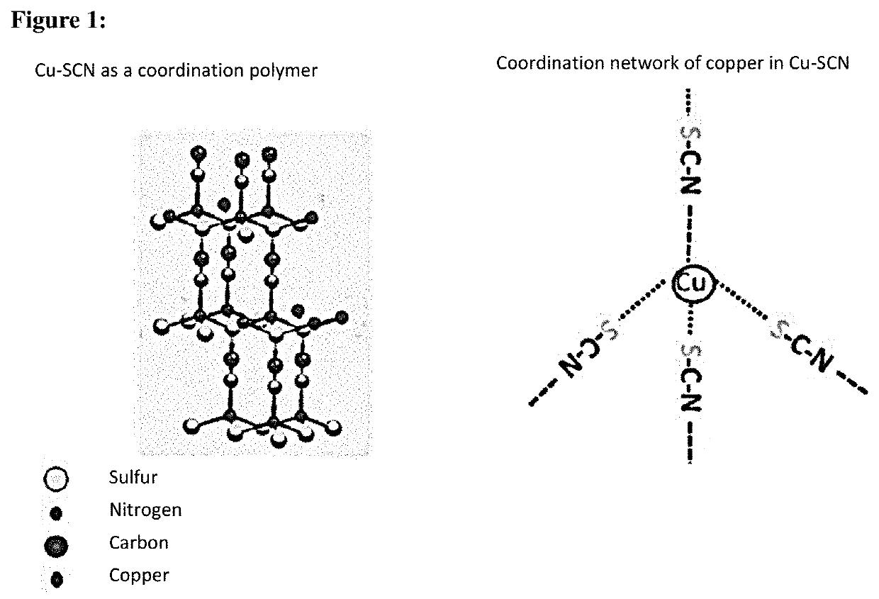
[0195]FIG. 1 shows a schematic representation of a CuSCN molecule.

DETAILED DESCRIPTION OF THE FIGURES

[0196]CuSCN is a pseudohalide and as a crystal structure forms a coordination network, see FIG. 1, left side. It belongs to the class of coordination polymers, i.e. inorganic polymers. The copper central atom coordinates on three sides with the sulfur atom of the thiocyanate group and on another side with the nitrogen atom of the thiocyanate group, see FIG. 1, right side.

[0197]It is noted that different alternatives to the described embodiments of the invention can be used to execute the invention and to arrive at the solution according to the invention. Thus, the component according to the invention as well as the system are not limited in their embodiments to the above described preferred embodiments. Rather, a pl...


PUM

PropertyMeasurementUnit
temperatureaaaaaaaaaa
temperaturesaaaaaaaaaa

Abstract

A method for producing a printable ink for an electronic component in which a transition metal-containing pseudohalide or chalcogenide is first complexed by a pyridine-like or thiol-like solvent, in order to improve or achieve solubility. Subsequently, by filtering and mixing with at least one solvent a printable ink is produced. The printable ink can be used to produce hole transport or electron blocking layers of electronic components.

Description

[0001]The invention relates to a method for producing a printable ink for an electronic component, wherein a transition metal-containing pseudohalide or chalcogenide is first complexed by a pyridine-like or thiol-like solvent, in order to improve or achieve solubility. Subsequently, by filtering and mixture with at least one solvent a printable ink is produced.[0002]The printable ink can be used to produce hole transport or electron blocking layers of electronic components, which shall also be covered by the invention.BACKGROUND AND STATE OF THE ART[0003]Organic light-emitting diodes (OLEDs) usually consist of a sandwich construction, with several layers of organic semiconducting materials between two electrodes. In particular, an OLED comprises one or more emitter layers (emitter layer EL), in which electromagnetic radiation, preferably in the visible range, is generated by a recombination of electrons with electron holes. The electrons and electron holes are each provided by a cat...

Claims


Application Information

Patent Timeline
Patent Type & Authority Applications(United States)
IPC IPC(8): C09D11/52C09D11/36C09D11/38
CPCC09D11/52H01L51/0004C09D11/38C09D11/36H10K50/15H10K50/18H10K71/13H10K71/40
Inventor RATAJCZAK, MARCINWOLOSZKA, MACIEJBARKOWSKI, PATRICK
Owner INURU GMBH
Why Eureka
Try Eureka