alpha-Ga2O3 SEMICONDUCTOR FILM

a technology of semiconductor film and alpha-ga2o3, which is applied in the direction of coating, semiconductor devices, chemical vapor deposition coating, etc., can solve the problems of epitaxial film, cracking problem, crystal defect formation, etc., and achieve the effect of fewer cracks

Pending Publication Date: 2022-07-28
NGK INSULATORS LTD
View PDF0 Cites 1 Cited by
  • Summary
  • Abstract
  • Description
  • Claims
  • Application Information

AI Technical Summary

Problems solved by technology

However, there is a problem that a crack or a crystal defect is formed when an α-Ga2O3 film is grown on different substrates.
When an InAlGaO semiconductor film, which is a mixed crystal of α-Ga2O3 and a different corundum material, is formed, in general, there is a cracking problem in an epitaxial film due to crystal growth on different substrates.

Method used


Image

  • alpha-Ga2O3 SEMICONDUCTOR FILM
  • alpha-Ga2O3 SEMICONDUCTOR FILM
  • alpha-Ga2O3 SEMICONDUCTOR FILM

Examples


example 1

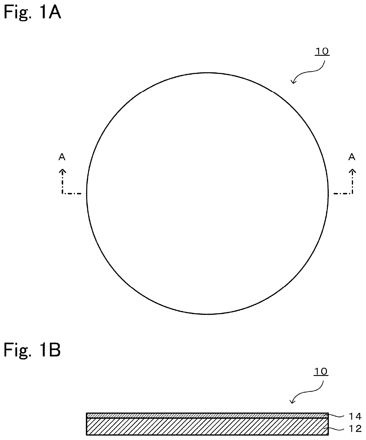
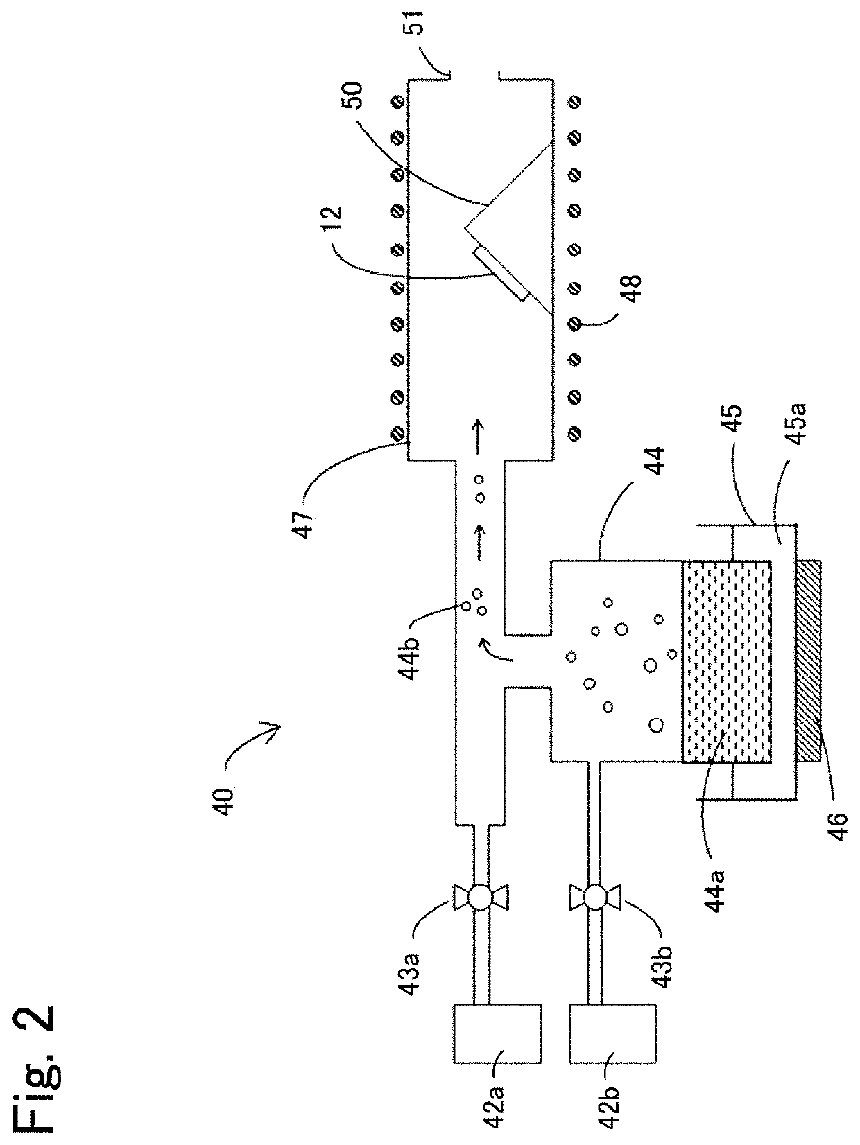
[0055]The mist CVD apparatus 40 illustrated in FIG. 2 was used to form an α-Ga2O3 film (semiconductor film) by the following method. The base substrate 12 was a commercial Cr2O3 single crystal (8 mm×8 mm, 0.5 mm in thickness, C-plane, no off-angle, hereinafter referred to as a Cr2O3 substrate).

[0056](1) Formation of α-Ga2O3 Film by Mist CVD Method

(1a) Adjustment of Raw Material Solution

[0057]An aqueous solution was adjusted at a gallium acetylacetonate concentration of 0.08 mol / L. The aqueous solution contained 1.5% by volume of 36% hydrochloric acid. Tin(II) chloride dihydrate (SnCl2.2H2O) was added to the aqueous solution such that the atomic ratio of tin to gallium was 0.2. The aqueous solution was used as the raw material solution 44a.

(1b) Preparation of Film Formation

[0058]Next, the raw material solution 44a was poured into the mist generation source 44 of the mist CVD apparatus 40 illustrated in FIG. 2. A Cr2O3 substrate was placed on the susceptor 50 as the base substrate 12...

example 2

[0085]An α-Ga2O3 film was formed in the same manner as in Example 1 except that the temperature in the quartz tube 47 at which the α-Ga2O3 film was formed by the mist CVD method was 430° C. Various evaluations were performed. The ratio R was 0.192. The entire film surface was observed in the same manner as in Example 1, and no cracks were observed. Application of a predetermined voltage to the Schottky barrier diode produced in the same manner as in Example 1 in the reverse direction caused a negligible leakage current, thus showing good device characteristics, as in Example 1.

example 3

[0086]An α-Ga2O3 film was formed in the same manner as in Example 1 except that a surface of a commercial Cr2O3 single crystal (8 mm×8 mm, 0.5 mm in thickness, C-plane, no off-angle) serving as a base substrate for film formation was ground to have a surface roughness Ra of 50 nm and the temperature in the quartz tube 47 at which the α-Ga2O3 film was formed by the mist CVD method was 430° C. Various evaluations were performed. The ratio R was 0.583. The entire film surface was observed in the same manner as in Example 1, and no cracks were observed. Application of a predetermined voltage to the Schottky barrier diode produced in the same manner as in Example 1 in the reverse direction caused a leakage current slightly larger than that in Example 1.


PUM

PropertyMeasurementUnit
wavelengthaaaaaaaaaa
wavelength rangeaaaaaaaaaa
blaze wavelengthaaaaaaaaaa

Abstract

An α-Ga2O3 semiconductor film according to the present invention has a measurement point (dark spot) with a maximum emission intensity A of not more than 0.6 times the average value X of top 5% of the maximum emission intensities A at all measurement points in intensity mapping of plane cathodoluminescence, wherein the maximum emission intensity A at each measurement point is determined in the wavelength range of 250 to 365 nm.

Description

BACKGROUND OF THE INVENTION1. Field of the Invention[0001]The present invention relates to an α-Ga2O3 semiconductor film.2. Description of the Related Art[0002]In recent years, gallium oxide (Ga2O3) has attracted attention as a semiconductor material. Gallium oxide is known to have five crystal forms of α, β, γ, δ, and E, among which α-Ga2O3 has a very large band gap of 5.3 eV and is expected as a power semiconductor material. Because α-Ga2O3 is a metastable phase, however, α-Ga2O3 has not been practically used as a single-crystal substrate and is generally formed on a sapphire substrate by heteroepitaxial growth.[0003]For example, PTL 1 discloses a semiconductor device including a base substrate with a corundum crystal structure, a semiconductor layer with a corundum crystal structure, and an insulating film with a corundum crystal structure, and describes an example in which an α-Ga2O3 film is formed as a semiconductor layer on a sapphire substrate. PTL 2 discloses a semiconductor...

Claims


Application Information

Patent Timeline
Patent Type & Authority Applications(United States)
IPC IPC(8): H01L29/06H01L29/24H01L29/04C23C16/40
CPCH01L29/0619H01L29/24H01L29/66969C23C16/40H01L29/045H01L29/872H01L21/02565H01L29/04H01L21/02628H01L21/0262H01L21/02414H01L21/0242H01L21/0243C23C16/4481
Inventor FUKUI, HIROSHIWATANABE, MORIMICHIYOSHIKAWA, JUN
Owner NGK INSULATORS LTD
Why Eureka
Try Eureka