Ultra-thin LED electrode assembly and method for manufacturing thereof

a technology of led electrodes and assembly, which is applied in the direction of basic electric elements, electrical equipment, semiconductor devices, etc., can solve the problems of difficult to manufacture an electrode assembly, difficult to implement led elements with ink, and more difficult to individually dispose of nano-leds

Pending Publication Date: 2022-09-29
KOOKMIN UNIV IND ACAD COOP FOUND
View PDF0 Cites 0 Cited by
  • Summary
  • Abstract
  • Description
  • Claims
  • Application Information

AI Technical Summary

Problems solved by technology

Displays and various light sources using micro-LEDs have advantages of high performance characteristics, a very long theoretical lifespan, and very high efficiency, but since the micro LEDs should be individually disposed on miniaturized electrodes in a limited region, when high unit cost, high process defect rate, and low productivity are considered, due to the limitations of process technology, it is difficult to manufacture an electrode assembly, which is implemented by disposing a micro-LED on the electrode with a pick and place technique, as a true high-resolution commercial display ranging from smartphones to TVs or as a light source having various sizes, shapes, and brightness.
Further, it is more difficult to individually dispose a nano-LED, which is smaller than the micro-LED, on an electrode by the pick and place technique as in the micro-LED.
However, in the disclosed technology, since the LED elements are aligned through the electric field, the LED elements should have a rod shape with a large aspec

Method used


Image

  • Ultra-thin LED electrode assembly and method for manufacturing thereof
  • Ultra-thin LED electrode assembly and method for manufacturing thereof
  • Ultra-thin LED electrode assembly and method for manufacturing thereof

Examples


preparation example 1

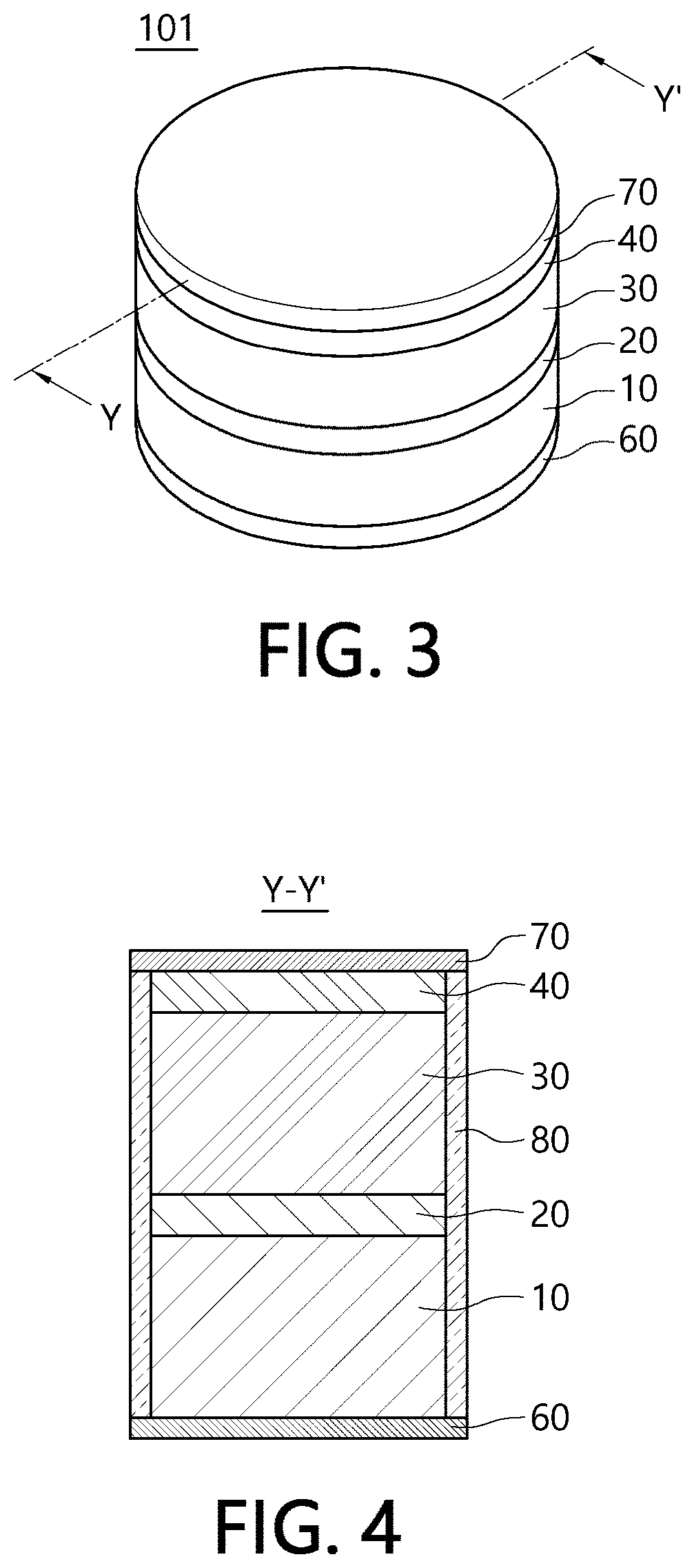
[0161]A common LED wafer (Epistar) in which an undoped n-type III-nitride semiconductor layer, an n-type III-nitride semiconductor layer doped with Si (a thickness of 4 μm), a photoactive layer (a thickness of 0.45 μm), and a p-type III-nitride semiconductor layer (a thickness of 0.05 μm) are sequentially stacked on a substrate was provided. ITO (a thickness of 0.15 μm) as a first electrode layer, SiO2 (a thickness of 1.2 μm) as a first mask layer, and Al (a thickness of 0.2 μm) as a second mask layer were sequentially deposited on the prepared LED wafer, and a spin on glass (SOG) resin layer onto which a pattern is transferred was transferred onto the second mask layer using nanoimprint equipment. Then, the SOG resin layer was cured using RIE, and the residual resin portion of the resin layer was etched through RIE to form a resin pattern layer. Then, the second mask layer was etched according to the pattern, using ICP and the first mask layer was etched using RIE. Next, after the ...

experimental example 1

[0164]Each of the LED element assemblies manufactured in Preparation Example 1 and Comparative Preparation Example 1 was put into acetone, and dispersed by being irradiated with ultrasonic waves under a 100 W condition, and then a dispersion state of the LED element was confirmed by measuring absorbance at 15 minute intervals for 2 hours, and a spectral area of the visible light region of 380˜780 nm was normalized using the measured results to be shown as an absorbance graph over time as shown in FIG. 20.

[0165]As can be seen from FIG. 20, it can be seen that an ultra-thin LED element according to Example 1 has excellent dispersion retention in the acetone solvent for a long time compared to the rod-type LED element according to Comparative Example 1.

example 1

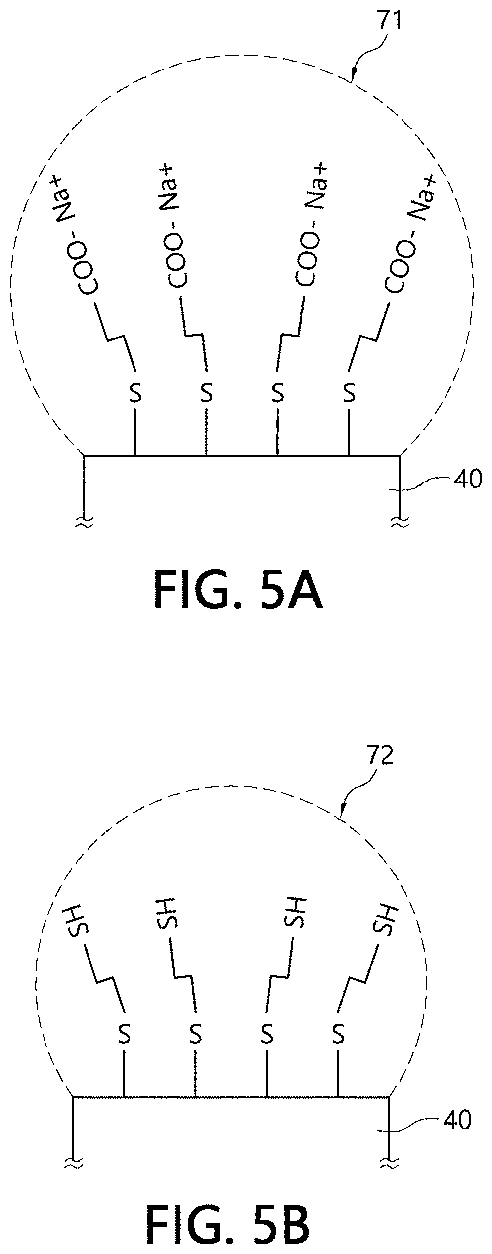
[0166]An ultra-thin LED element aggregate manufactured in the same manner as the ultra-thin LED element manufactured in Preparation Example 1, and further formed with a Ti / Au layer (a thickness of 10 nm / 100 nm) as an electrode layer on the first electrode layer and then formed with a bonding layer with exposed thiol groups by treating 1,2-ethanedithiol on the Ti / Au layer before separating from the LED wafer through ultrasonic waves was prepared

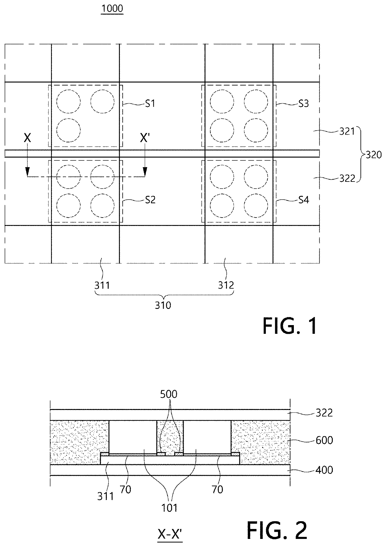
[0167]Then, the ultra-thin LED elements were assembled upright on the first electrodes for a predetermined time by immersing a lower electrode line including the first electrodes in an ink composition containing the ultra-thin LED element aggregate. At this time, an ultra-thin LED element having a diameter of 750 nm and a height of 1.1 μm was used as the ultra-thin LED element. Then, after forming SiO2 (1.4 μm to 1.6 μm) as an insulating layer for serving as an insulator, an ultra-thin LED electrode aggregate having a lateral length and a long...


PUM


Abstract

The present disclosure relates to a light-emitting diode (LED) electrode assembly, and more specifically, to an ultra-thin LED electrode assembly and a manufacturing method thereof.

Description

CROSS-REFERENCE TO RELATED APPLICATION[0001]This application claims priority to and the benefit of Korean Patent Application No. 10-2021-0039000, filed on Mar. 25, 2021, the disclosure of which is incorporated herein by reference in its entirety.BACKGROUND1. Field of the Invention[0002]The present disclosure relates to a light-emitting diode (LED) electrode assembly, and more specifically, to an ultra-thin LED electrode assembly and a manufacturing method thereof.2. Discussion of Related Art[0003]A micro light-emitting diode (LED) and a nano LED can realize an excellent feeling of color and high efficiency, and are made of eco-friendly materials, and thus are being used as core materials for various light sources or displays. In line with these market conditions, recently, studies for developing a nanocable LED coated with a shell through a new manufacturing process or a new nanorod LED structure are proceeding. Further, research on a protective film material for achieving high effi...

Claims


Application Information

Patent Timeline
IPC IPC(8): H01L33/38H01L33/32H01L33/40H01L33/00
CPCH01L33/382H01L33/32H01L33/40H01L33/005H01L2933/0016H01L33/36H01L33/20H01L33/0075H01L33/16H01L33/0093H01L33/62H01L33/44H01L2933/0008
Inventor DO, YOUNG RAG
Owner KOOKMIN UNIV IND ACAD COOP FOUND
Why Eureka
Try Eureka