

High throughput multi-electron beam system
a multi-electron beam, high-throughput technology, applied in the direction of electrical equipment, electric discharge tubes, basic electric elements, etc., can solve the problems of affecting the electrical parameters of the device, the operation of semiconductor manufacturing processes closer to the limitation of the performance capability of the process, and the failure to detect defects of decreasing siz
- Summary
- Abstract
- Description
- Claims
- Application Information
AI Technical Summary
Benefits of technology
Problems solved by technology
Method used
Image

Examples
Embodiment Construction
[0044]Although claimed subject matter will be described in terms of certain embodiments, other embodiments, including embodiments that do not provide all of the benefits and features set forth herein, are also within the scope of this disclosure. Various structural, logical, process step, and electronic changes may be made without departing from the scope of the disclosure. Accordingly, the scope of the disclosure is defined only by reference to the appended claims.
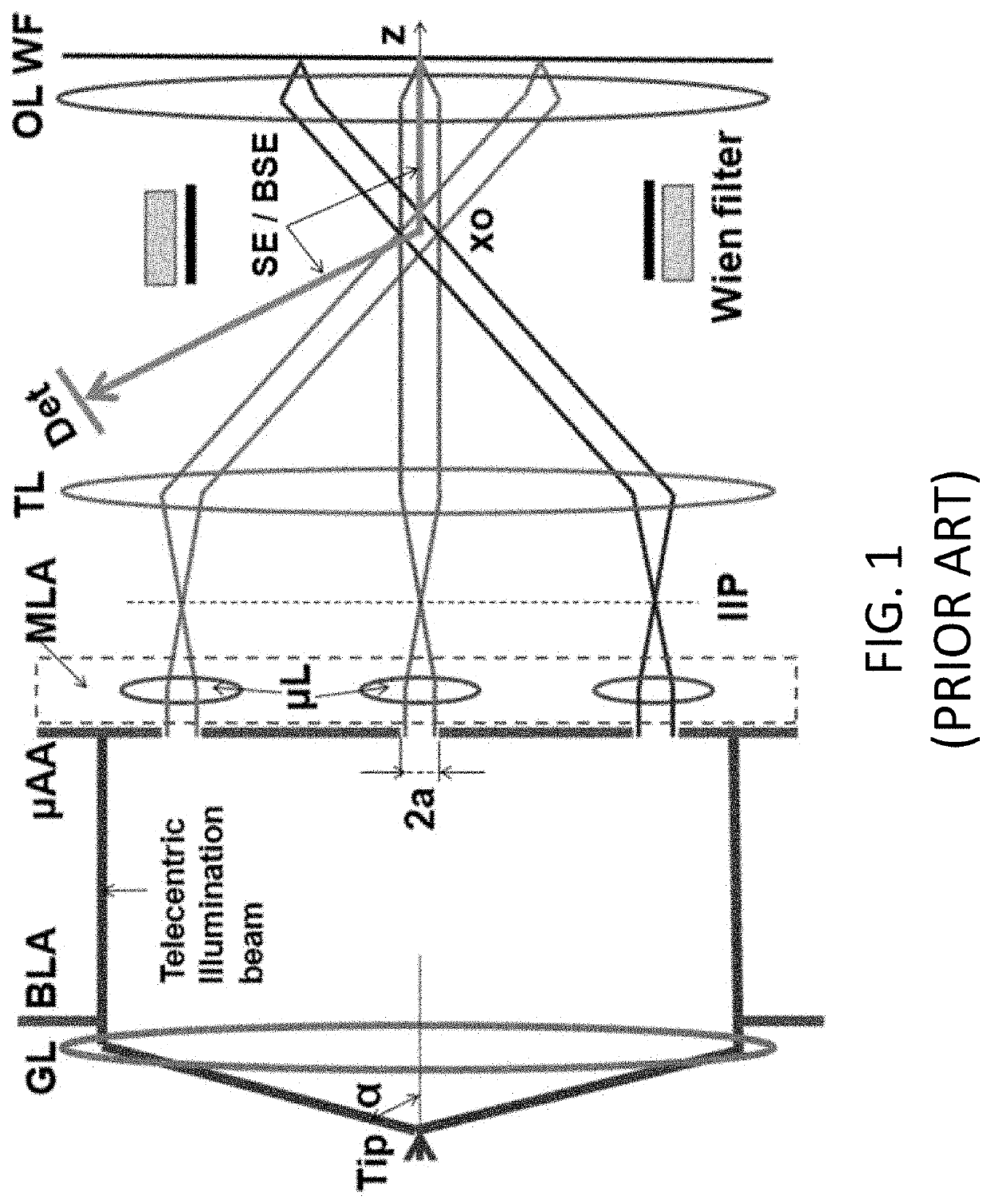
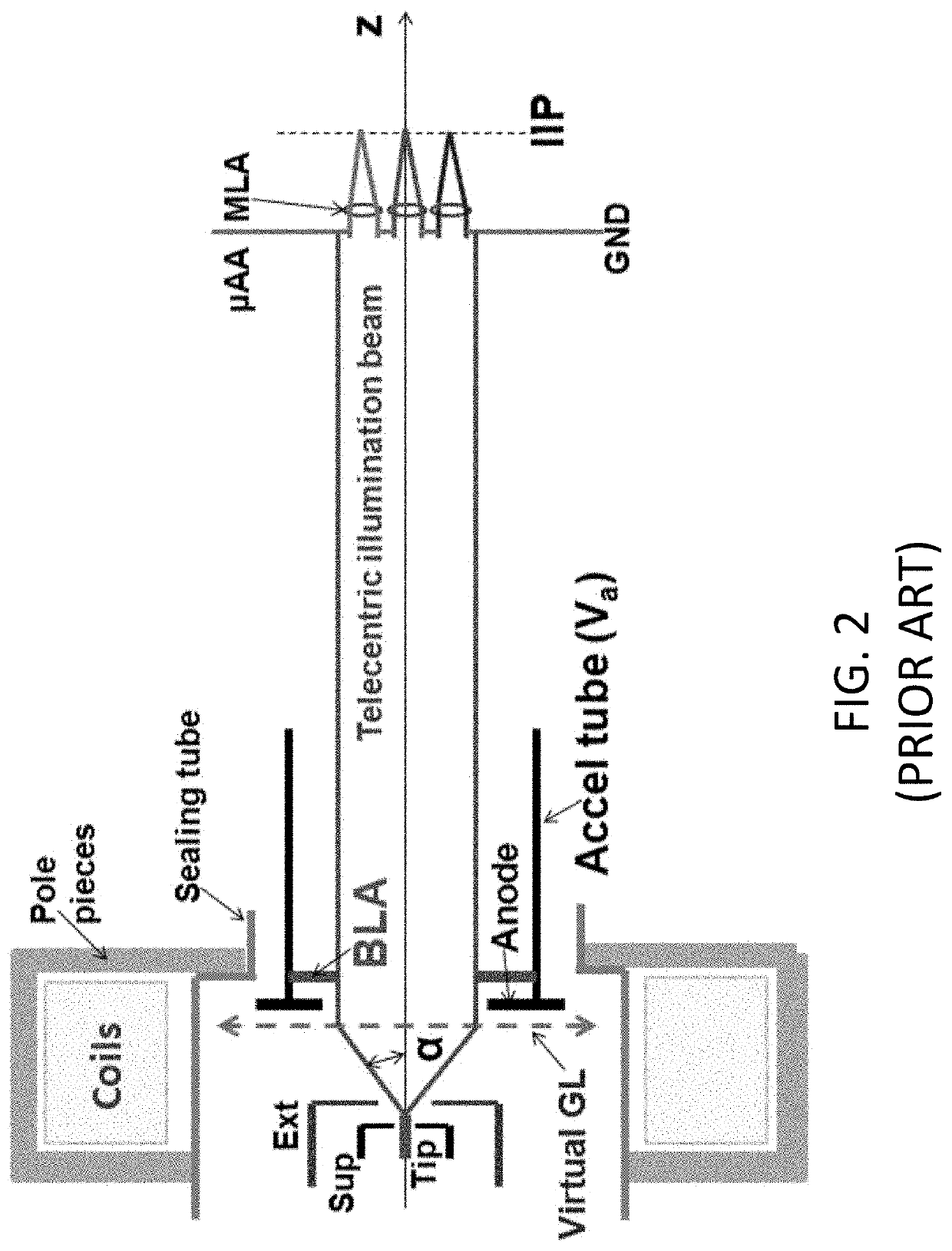
[0045]In the embodiments disclosed herein, a divergent illumination beam with a smaller emission angle is focused into a telecentric illumination beam by a collimated lens. This not only reduces the gun lens spherical aberration, but also removes the off-axis blurs and distortion in a micro lens array and can raise the throughput by 5× or more. The spherical aberration from the gun lens can be responsible for degradation of the beamlet resolution when increasing the throughput (or with increasing the number of total beaml...
PUM
 Abstract
Description
Claims
Application Information