Substrate for an electronic device and method for producing the same

a technology for electronic devices and substrates, applied in the direction of crystal growth process, after-treatment details, semiconductor/solid-state device details, etc., can solve the problems of easy increase in warp and plastic deformation, difficult to produce nitride wafers, and large amount of warp over 50 m, so as to achieve suppressed warp and inexpensive production

Pending Publication Date: 2022-11-17
SHIN-ETSU HANDOTAI CO LTD
View PDF0 Cites 1 Cited by
  • Summary
  • Abstract
  • Description
  • Claims
  • Application Information

AI Technical Summary

Benefits of technology

[0036]Such a substrate for an electronic device and method for producing the same include a hard base wafer including CZ silicon having a resistivity of 0.1 Ωcm or lower and a crystal orientation of <100>, so that the warping of the substrate for an electronic device can be suppressed. In addition, since a bond wafer having a crystal orientation of <111> is joined on the base wafer, a favorable nitride semiconductor film can be formed. Furthermore, since wafers having diff

Problems solved by technology

It is difficult to produce a nitride wafer having a nitride semiconductor grown on a substrate for such devices, and a sapphire substrate or an SiC substrate is used as the substrate.
However, due to stress caused by a difference in lattice constant or a difference in thermal expansion coefficient, an

Method used


Image

  • Substrate for an electronic device and method for producing the same

Examples


example 1

[0069]A base wafer (diameter: 150 mm) having a thickness of 500 μm and a base wafer (diameter: 150 mm) having a thickness of 1000 μm were prepared from (100) plane CZ silicon substrates each having a resistivity of 0.1 Ωcm or lower and an oxygen concentration of 1×10¹⁸ atoms / cm3 (ASTM'79) or lower (resistivity: 0.007 Ωcm, oxygen concentration: 7×10¹⁷ atoms / cm3). In addition, for bonding, two bond wafers (diameter: 150 mm) each having a thickness of 500 μm were prepared from (111) plane CZ silicon substrates each having a resistivity of 0.1 Ωcm or lower and an oxygen concentration of 1×10¹⁸ atoms / cm3 (ASTM'79) or lower (resistivity: 0.007 Ωcm, oxygen concentration: 7×10¹⁷ atoms / cm3).

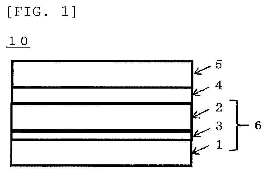
[0070]Next, substrates for an electronic device like the substrate shown in FIG. 1 were fabricated in the following manner. The two base wafers 1 were each subjected to thermal oxidation (thickness: 1 μm), and the two bond wafers 2, having been polished on both sides, were each subjected to thermal oxidat...

example 2

[0071]A base wafer (diameter: 150 mm) having a thickness of 500 μm and a base wafer (diameter: 150 mm) having a thickness of 1000 μm were prepared from (100) plane CZ silicon substrates each having a resistivity of 0.1 Ωcm or lower and an oxygen concentration of 1×10¹⁸ atoms / cm3 (ASTM'79) or lower (resistivity: 0.007 Ωcm, oxygen concentration: 7×10¹⁷ atoms / cm3). In addition, for bonding, two bond wafers (diameter: 150 mm) each having a thickness of 500 μm were prepared from (111) plane CZ silicon substrates of 1000 Ωcm or higher doped with nitrogen at a high concentration (8×10¹⁴ atoms / cm3, 5000 Ωcm).

[0072]Next, substrates for an electronic device like the substrate shown in FIG. 1 were fabricated in the following manner. The two base wafers 1 were subjected to thermal oxidation (thickness: 1 μm), and the two bond wafers 2, having been polished on both sides, were subjected to thermal oxidation (thickness: 1 μm). Then, through a bonding process, a bonding heat treatment was performe...

example 3

[0073]A base wafer (diameter: 150 mm) having a thickness of 500 μm and a base wafer (diameter: 150 mm) having a thickness of 1000 μm were prepared from (100) plane CZ silicon substrates each having a resistivity of 0.1 Ωcm or lower and an oxygen concentration of 1×10¹⁸ atoms / cm3 (ASTM'79) or lower (resistivity: 0.007 Ωcm, oxygen concentration: 7×10¹⁷ atoms / cm3). In addition, for bonding, two bond wafers (diameter: 150 mm) each having a thickness of 500 μm were prepared from (111) plane FZ silicon substrates of 1000 Ωcm or higher doped with nitrogen at a high concentration (8×10¹⁴ atoms / cm3, 5000 Ωcm).

[0074]The base wafers 1 were subjected to thermal oxidation (thickness: 1 μm), and the bond wafers 2, having been polished on both sides, were subjected to thermal oxidation (thickness: 1 μm). Then, through a bonding process, a bonding heat treatment was performed at 1150° C. for 2 hours. Subsequently, the bond wafers of the bonded substrates were ground and polished to make the thickne...


PUM


Abstract

The present invention is a substrate for an electronic device, including a nitride semiconductor film formed on a joined substrate including a silicon single crystal, where the joined substrate has at least a bond wafer including a silicon single crystal joined on a base wafer including a silicon single crystal, the base wafer includes CZ silicon having a resistivity of 0.1 Ωcm or lower and a crystal orientation of <100>, and the bond wafer has a crystal orientation of <111>. This provides a substrate for an electronic device, having a suppressed warp.

Description

TECHNICAL FIELD[0001]The present invention relates to: a substrate for an electronic device; and a method for producing the same.BACKGROUND ART[0002]Nitride semiconductors, including GaN and AlN, can be used for fabricating high electron mobility transistors (HEMT) and electronic devices with a high breakdown voltage that use two-dimensional electron gas.[0003]It is difficult to produce a nitride wafer having a nitride semiconductor grown on a substrate for such devices, and a sapphire substrate or an SiC substrate is used as the substrate. However, in order to suppress costs for achieving a larger diameter and costs for a substrate, epitaxial growth by vapor deposition on a silicon substrate is employed. When an epitaxially grown film is fabricated by vapor deposition on a silicon substrate, a substrate with a larger diameter can be used compared to when a sapphire substrate or an SiC substrate is used, so that the productivity of devices is high, and there are advantages regarding...

Claims


Application Information

Patent Timeline
IPC IPC(8): H01L21/18H01L21/02H01L21/762C30B29/06H01L23/00
CPCH01L21/185H01L21/02381H01L21/76254H01L21/02002H01L21/02389C30B29/06H01L23/562H01L21/02H01L27/12C30B33/06
Inventor HAGIMOTO, KAZUNORIGOTO, SHOUZABURO
Owner SHIN-ETSU HANDOTAI CO LTD
Why Eureka
Try Eureka