Electrode with domes for plasma focusing
a plasma focusing and electrolytic technology, applied in the direction of plasma technique, chemical vapor deposition coating, coating, etc., can solve the problems of limiting the use of plasma-driven processes to fabricating larger, coarser structures, and requiring a lower processing pressure, so as to reduce the escape of reactive species and be inexpensively integrated into existing plasma-driven reactors
- Summary
- Abstract
- Description
- Claims
- Application Information
AI Technical Summary
Benefits of technology
Problems solved by technology
Method used
Image
Examples
example 2
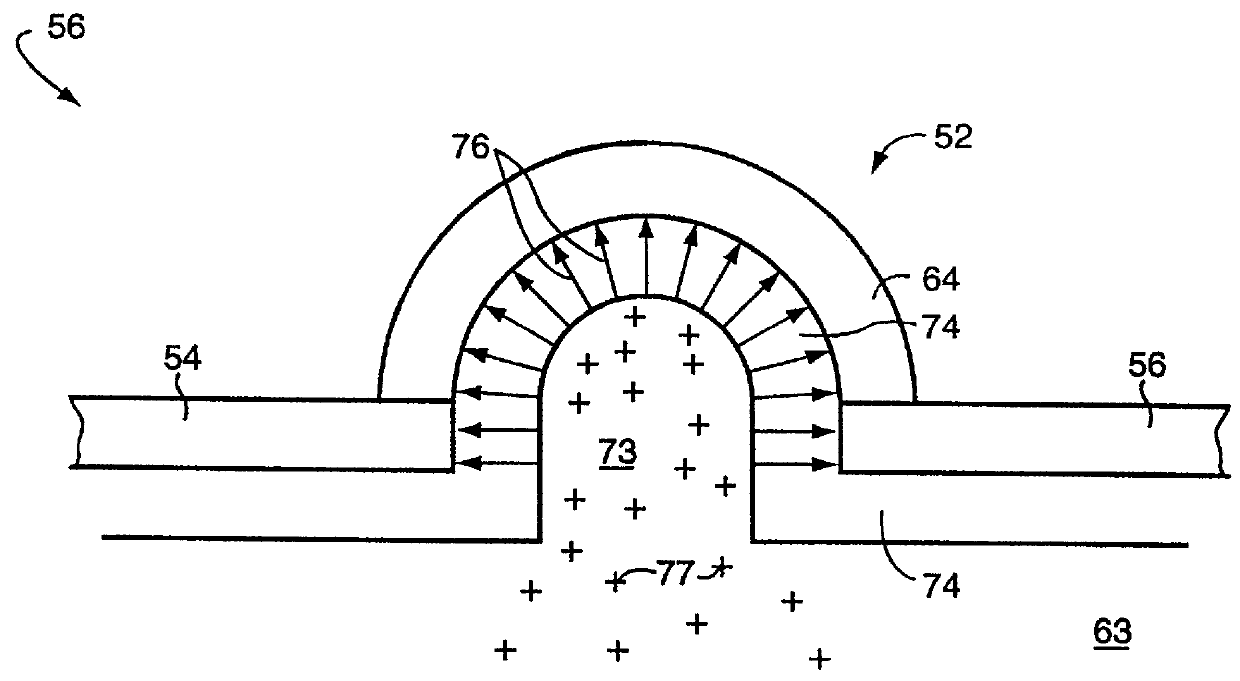
A 200-mm-diameter silicon wafer covered by a 1.8 .mu.m blanket of CVD-grown oxide, similar to that used in the run described for Example 1, was mounted at the lower electrode. The anode 120 featured seven domes 52 placed among cylindrical holes 124 in the arrangement illustrated in FIG. 7. Thus, about 37% of the featured area within curve 128 was covered by domes 52 and the remainder covered by cylindrical holes 124. The domes were each formed from a 15 mm cylindrical hole covered with a 7.5 mm radius aluminum hemisphere as depicted in FIG. 3. The wafer was subjected to a two-minute etch under the process conditions indicated above. After the etch sequence, the thickness of the remaining oxide was measured using a profilometer over a 88-mm-diameter central region centered on the part of the wafer located directly under the center feature 130. The surface profile revealed "craters", indicating local enhancement of the etch rate, in a spatial arrangement corresponding to the arrangeme...
example 3
A 200-mm-diameter silicon wafer covered by a 1.8 .mu.m blanket of CVD-grown oxide, in turn covered by a 1-.mu.m layer of resist, was mounted at the lower electrode. Defined in the resist layer was a distribution of 0.35 .mu.m-wide and 0.50 .mu.m-wide contact openings. The anode 130 featured nineteen domes 52 placed at adjacent feature sites in the arrangement illustrated in FIG. 9, so that all 19 features bounded by the curve 134 were domes 52. All of the other features were cylindrical holes 136. No special care was taken to position the contact openings under domes. The wafer was subjected to a three-minute etch according to the processing conditions indicated above. After the etch sequence, the contact openings were examined and the etch rates calculated from the depth of the contact holes under the openings. The average of etch rates at contact openings outside the central region of the wafer under the portion of the anode within curve 134 was about 5000 .ANG. / min. The average o...
PUM
| Property | Measurement | Unit |
|---|---|---|
| Pressure | aaaaa | aaaaa |
| Diameter | aaaaa | aaaaa |
| Density | aaaaa | aaaaa |
Abstract
Description
Claims
Application Information


