Single crystal SiC and a method of producing the same

a single crystal, crystal sic technology, applied in the field of single crystal sic, can solve the problems of low crystal growth rate, leakage current, and difficulty in singly obtaining a large-size single crystal

Inactive Publication Date: 2000-04-25
NISSIN ELECTRIC CO LTD
View PDF3 Cites 46 Cited by
  • Summary
  • Abstract
  • Description
  • Claims
  • Application Information

AI Technical Summary

Problems solved by technology

In the Achison method of the above-described conventional production methods, however, a single crystal is grown slowly over a long time period, so that the crystal growth rate is very low.
Thus, it is difficult to singly obtain a large-size single crystal.
Such pin holes are called micropipe defects and cause a leakage current when a semiconductor device is fabricated.
Accordingly, there exists a problem in that single crystal SiC having sufficiently good quality cannot be obtained.
This blocks a practical use of SiC which has superior characteristics as compared with other existing semiconductor materials such as Si and GaAs as described above.

Method used


Image

  • Single crystal SiC and a method of producing the same
  • Single crystal SiC and a method of producing the same
  • Single crystal SiC and a method of producing the same

Examples


Embodiment Construction

Hereinafter, an embodiment of the invention will be described with reference to the drawings.

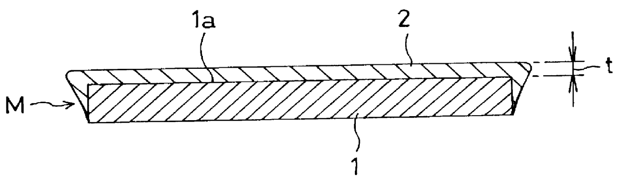
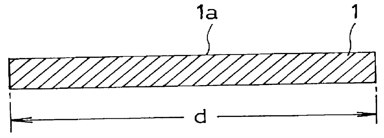
FIGS. 1 to 4 are views illustrating the method of producing single crystal SiC according to the invention, in the sequence of production steps. In FIG. 1, 1 denotes a single crystal hexagonal .alpha.-SiC substrate (6H type or 4H type) which is processed so as to have a disk-like shape of a diameter d of about 25 mm. The surface 1a of the single crystal .alpha.-SiC substrate 1 is ground or polished so as to remove physical unevenness. Specifically, the surface 1a is adjusted so as to have a surface roughness which is equal to or lower than 2,000 angstroms RMS, preferably equal to or lower than 1,000 angstroms RMS, and more preferably in the range of 100 to 500 angstroms.

Thereafter, on the surface 1a of the single crystal .alpha.-SiC substrate 1, a polycrystalline .alpha.-SiC film 2 is grown as shown in FIG. 2 by thermal chemical vapor deposition (hereinafter referred to as thermal CVD) under ...


PUM

PropertyMeasurementUnit
surface roughnessaaaaaaaaaa
temperatureaaaaaaaaaa

Abstract

The surface 1a of a single crystal alpha -SiC substrate 1 is adjusted so as to have a surface roughness equal to or lower than 2,000 angstroms RMS, and preferably equal to or lower than 1,000 angstroms RMS. On the surface 1a of the single crystal alpha -SiC substrate 1, a polycrystalline alpha -SiC film 2 is grown by thermal CVD to form a complex is placed in a porous carbon container and the carbon container is covered with alpha -SiC powder. The complex is subjected to a heat treatment at a temperature equal to or higher than a film growing temperature, i.e., in the range of 1,900 to 2,400 DEG C. in an argon gas flow, whereby single crystal alpha -SiC is integrally grown on the single crystal alpha -SiC substrate 1 by crystal growth and recrystallization of the polycrystalline alpha -SiC film 2. It is possible to stably and efficiently produce single crystal SiC of a large size which has a high quality and in which any crystal nucleus is not generated.

Description

1. Field of the InventionThe present invention relates to single crystal SiC and a method of producing the same, and more particularly to single crystal SiC which is used as a semiconductor substrate wafer for a light-emitting diode, an X-ray optical element such as a monochromatic sorter, a high-temperature semiconductor electronic element, and a power device, and also to a method of producing the single crystal SiC.2. Description of the Prior ArtSiC (silicon carbide) is superior in heat resistance and mechanical strength, and also has good resistance to radiation. In addition, it is easy to perform the valence control of electrons and holes by doping an impurity. Moreover, SiC has a wide band gap (for example, single crystal 6H-SiC has a band gap of about 3.0 eV, and single crystal 4H-SiC has a band gap of 3.26 eV). Therefore, it is possible to realize a large capacity, a high frequency, a high dielectric strength, and a high resistance to environments which cannot be realized by ...

Claims


Application Information

Patent Timeline
Patent Type & Authority Patents(United States)
IPC IPC(8): C30B25/02C30B1/02C30B29/36H01L33/16H01L33/34
CPCC30B25/02C30B29/36Y10T428/12528
Inventor TANINO, KICHIYAHIRAMOTO, MASANOBU
Owner NISSIN ELECTRIC CO LTD
Why Eureka
Try Eureka