Process for forming zinc oxide film and processes for producing semiconductor device substrate and photo-electricity generating device using the film

a technology of zinc oxide film and photoelectricity generating device, which is applied in the direction of final product manufacture, sustainable manufacturing/processing, liquid/solution decomposition chemical coating, etc., can solve the problems of lowering the weather resistance of the photoelectricity generating device using the zinc oxide film, the effect of reducing the production yield

Inactive Publication Date: 2000-08-22
CANON KK
View PDF2 Cites 74 Cited by
  • Summary
  • Abstract
  • Description
  • Claims
  • Application Information

AI Technical Summary

Problems solved by technology

Further, in the resultant zinc oxide film, remarkable anomalous growth of the deposited (precipitated) crystal of ZnO has been confirmed, thus leading to defects of a photo-electricity generating device using the zinc oxide film to lower a production yield thereof.
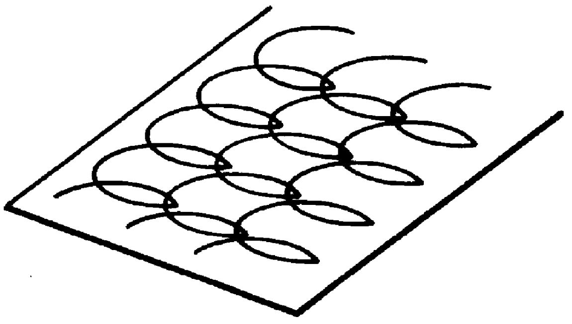
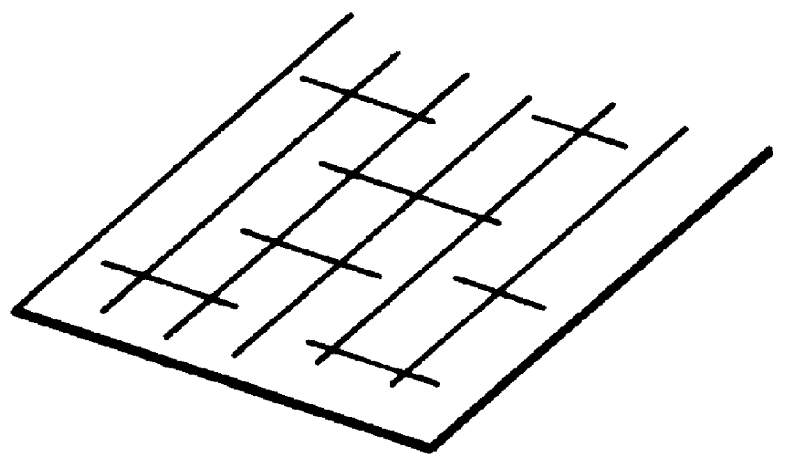
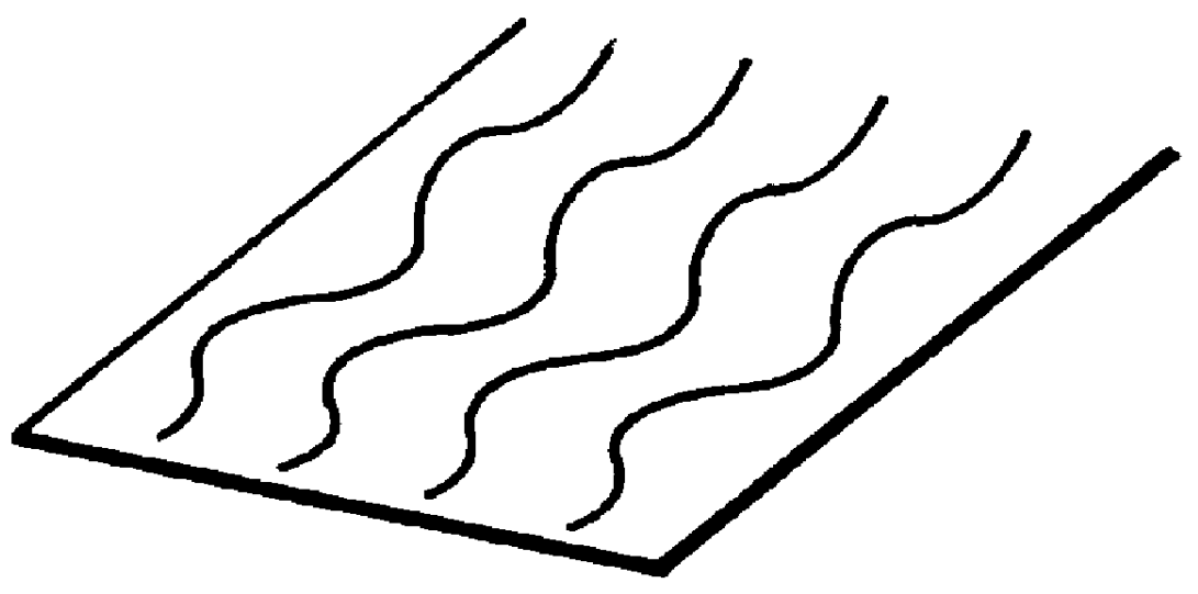
These problems have similarly be found in the case where the Ra(Y) exceeds 600 nm since the resultant uneven surface have remarkably large irregularities although the uneven surface includes the linear projections.
As a result, the photo-electricity

Method used


Image

  • Process for forming zinc oxide film and processes for producing semiconductor device substrate and photo-electricity generating device using the film
  • Process for forming zinc oxide film and processes for producing semiconductor device substrate and photo-electricity generating device using the film
  • Process for forming zinc oxide film and processes for producing semiconductor device substrate and photo-electricity generating device using the film

Examples


example 2

A photo-electricity generating device was prepared in the same manner as in Example 1 except that the BA finish of the cold-rolled stainless steel slab (SUS 430) was changed to a so-called 2D finish wherein the stainless steel slab was subjected to heat treatment and acid washing, followed by light rolling with a roll having a small surface roughness and that the etching treatment with the hydrofluoric acid-nitric acid mixture was not effected.

The 2D-finished stainless steel plate (before the overlying layers were formed) was subjected to measurement of center-line average surface roughnesses Ra(X) and Ra(Y) in the same manner as in Example 1, whereby the stainless steel plate was found to have an uneven surface including linear projections and having an Ra(X) of 65 nm and Ra(Y) of 200 nm.

example 3

A photo-electricity generating device was prepared in the same manner as in Example 1 except that the BA finish of the cold-rolled stainless steel slab (SUS 430) was changed to a so-called 2D finish similarly as in Example 2 and that the etching treatment was performed for 1 minute with a hydrofluoric acid-nitric acid mixture (HF:HNO.sub.3 :H.sub.2 O=1:3:5).

The stainless steel plate (before the overlying layers were formed) was subjected to measurement of center-line average surface roughnesses Ra(X) and Ra(Y) in the same manner as in Example 1, whereby the stainless steel plate was found to have an uneven surface including linear projections and having an Ra(X) of 300 nm and Ra(Y) of 600 nm.

example 4

A photo-electricity generating device was prepared in the same manner as in Example 1 except that (1) the BA finish of the cold-rolled stainless steel slab (SUS 430) was changed to a so-called 2B finish wherein a cold-rolled austenitenic stainless steel slab (SUS 304) was subjected to heat treatment and acid washing, followed by light cold rolling, that (2) the 1 .mu.m-thick Ag layer was changed to a 0.5 .mu.m-thick copper (Cu) layer, and that (3) the zinc oxide film forming conditions were changed as described below.

The 0.5 .mu.m-thick Cu layer was formed by electroplating with a plating bath comprising copper pyrophosphate (80 g / l), potassium pyrophosphate (300 g / l), ammonia water (6 ml / l), potassium nitrate (10 g / l) under conditions including an anode of a Cu plate, a cathode of the stainless steel plate, a plating temperature of 50-60.degree. C., a pH of 8.2-8.8 and an anode current density of 30 mA / cm.sup.2.

The 1 .mu.m-thick zinc oxide film was formed in the same manner as in E...


PUM

PropertyMeasurementUnit
Nanoscale particle sizeaaaaaaaaaa
Lengthaaaaaaaaaa

Abstract

A process for forming a zinc oxide film including immersing an electroconductive substrate having a surface including a plurality of linear projections in an aqueous solution containing at least nitrate ions and zinc ions to form a zinc oxide film on the electroconductive substrate by a liquid-phase deposition. The plurality of linear projections may preferably provide an uneven surface which has a center-line average surface roughness Ra(X) of 15-300 nm when scanned in a direction parallel to the linear projections, a center line average surface roughness Ra(Y) of 20-600 nm when scanned in a direction perpendicular to the linear projections, and an Ra(X)/Ra(Y) ratio of at most 0.8. The thus formed zinc oxide film is provided with an uneven surface suitable for an optical-confinement layer of a photo-electricity generating device excellent in photoelectric performances.

Description

FIELD OF THE INVENTION AND RELATED ARTThe present invention relates to a process for forming a zinc oxide film through deposition in liquid phase so as to have an uneven surface suitable for obtaining a light-confining effect and relates to processes for producing a substrate for a semiconductor device and an photo-electricity generating device using the zinc oxide film.In a process for producing an electro-electricity generating device, there has been known that a reflection layer of, e.g., metal is formed on the back side of an semiconductor layer in order to improve a light-collection efficiency of the photo-electricity generating device on a long wavelength. Further, there has also been known that a transparent electroconductive layer having an uneven surface is formed between the reflection layer and the semiconductor layer to obtain a light-confining (optical confinement) effect that an optical distance (optical path) of reflected light is prolonged to obtain an effect of supp...

Claims


Application Information

Patent Timeline
IPC IPC(8): C25D9/08C25D9/00C25D5/10C23C18/16C23C18/52H01L31/0236H01L31/075H01L31/06H01L31/18H01L31/20H01L31/076
CPCC23C18/52C25D5/10C25D9/08H01L31/076H01L31/1824H01L31/1884H01L31/202H01L31/204H01L31/206H01L31/02363Y02E10/545Y02E10/548C25D5/627Y02P70/50
Inventor MATSUYAMA, JINSHO
Owner CANON KK
Why Eureka
Try Eureka