Reactive preclean prior to metallization for sub-quarter micron application

a technology of pre-metallization and sub-quarter microns, which is applied in the direction of vacuum evaporation coating, chemical vapor deposition coating, coating, etc., can solve the problems of void formation within the features, increased difficulty in cleaning the features, and large aspect ratio of features

Inactive Publication Date: 2000-08-22
APPLIED MATERIALS INC
View PDF10 Cites 230 Cited by
  • Summary
  • Abstract
  • Description
  • Claims
  • Application Information

AI Technical Summary

Problems solved by technology

The decrease in width of the features results in larger aspect ratios for the features and increased difficulty in cleaning the features prior to filling the features with metal or other materials.
Failure to clean the features can result in void formation within the features or an increase in the resistance of the features.
Therefore, there is a great amount of ongoing effort being directed at cleaning small features having high aspect ratios, especially where the ratio of feature height to width is 4:1 or larger.
The presence of native oxides and other contaminants within a small feature typically results in voids by promoting uneven distribution of the depositing metal.
Oxygen exposure occurs when moving substrates between processing chambers at atmospheric conditions, or when the small amount of oxygen remaining in a vacuum chamber contacts the wafer / film layer, or when a layer is damaged by etching.
The native oxide and other contaminants create regions on the substrate which interfere with film formation, by creating regions where film growth is stunted.
The presence of native oxides and other contaminants also can increase the via / contact resistance and can reduce the electromigration resistance of small features.
The contaminants can diffuse into the dielectric layer, the sublayer, or the deposited metal and alter the performance of devices which include the small features.
However, sputter etch processes can damage silicon layers by physical bombardment, sputter deposit Si / SiO.sub.2 onto sidewalls of the features, and sputter metal sublayers, such as aluminum or copper, onto sidewalls of the features.
For small features having larger aspect ratios, sputter etch processes have not been as effective in removing contaminants within the features, thereby compromising the performance of the devices which are formed.
Preclean by sputter etch process is particularly unsuitable for features with copper substrate.
However, the addition of wet chemical cleaning steps to remove trace amounts of contaminants from the features substantially increases the overall process time for metallization.
The process does not avoid resputtering of materials from the bottom to the sidewalls of the contact hole.
However, addition of H.sub.2 to Ar in the cleaning process does not completely eliminate resputtering of materials within the features.
For sub-quarter micron features having high aspect ratios, resputtering of material from the bottom to the sidewalls of the feature during dry cleaning results in a significant narrowing of the feature and a corresponding increase in resistance of the feature which impairs device performance.
The known dry cleaning processes are not effective in removing contaminants from the features without redepositing material on the sidewalls of the features.

Method used


Image

  • Reactive preclean prior to metallization for sub-quarter micron application
  • Reactive preclean prior to metallization for sub-quarter micron application
  • Reactive preclean prior to metallization for sub-quarter micron application

Examples


example

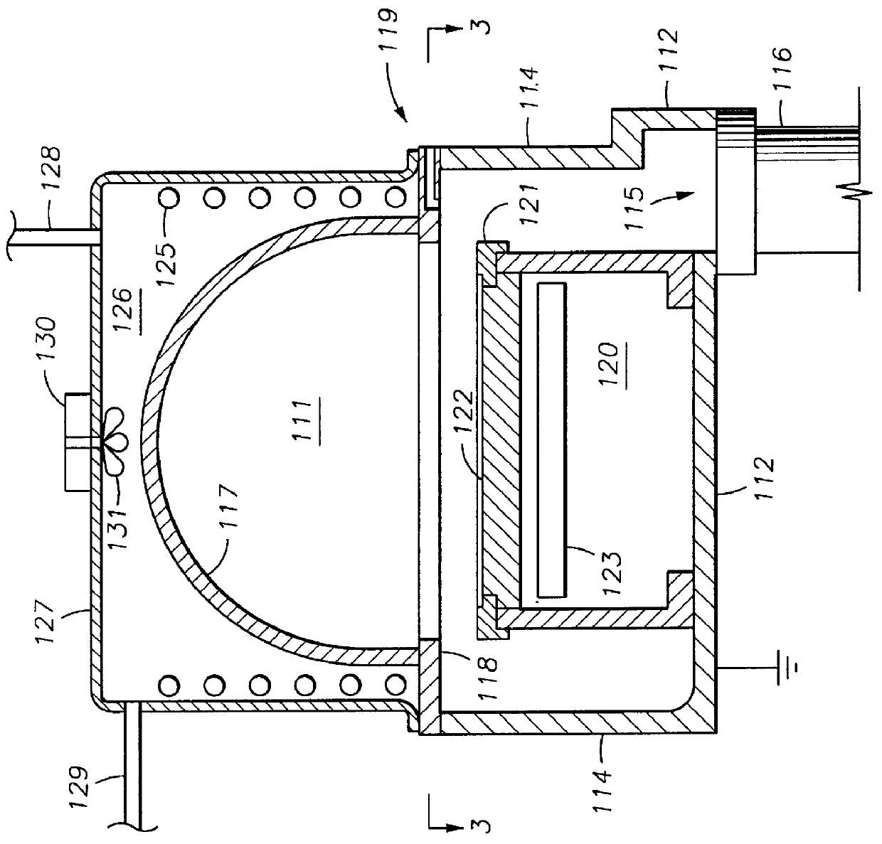
The precleaning steps of the present invention have been combined in the chamber shown in FIGS. 2-4 to successfully clean features etched in a dielectric layer having a copper sublayer prior to filling of the features with a Cu or Al plug. The chamber was stabilized for 5 seconds at a pressure of 5-20 mTorr with a mixture of 90% H.sub.2 and 10% He, Ar, or N.sub.2. The features were then cleaned for 60 seconds by applying 300 W of 400 KHz RF power to the coil and 10 W of RF power (13.56 MHZ) to the pedestal. These process conditions (i.e. with very low bias) can chemically reduce CuO without sputtering of the Cu sublayer onto the sidewalls. Similar treatment can also be used for Si or TiSi.sub.x sublayers at higher temperatures.

Integrated Processing System

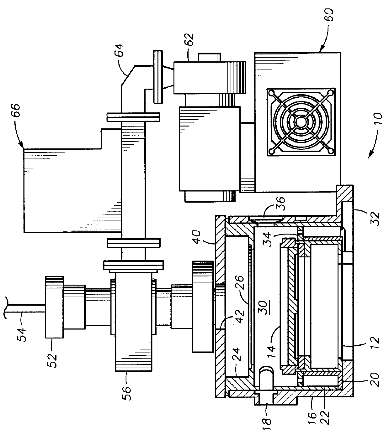
The precleaning process of this invention is conducted in the dedicated precleaning chamber as described above, or done in situ in the barrier layer chamber. The precleaning chamber is preferably integrated with other metallization ...


PUM

PropertyMeasurementUnit
pressureaaaaaaaaaa
microwave poweraaaaaaaaaa
pressureaaaaaaaaaa

Abstract

The present invention generally provides a precleaning process prior to metallization for submicron features on substrates. The method includes cleaning the submicron features with radicals from a plasma of a reactive gas such as oxygen, a mixture of CF4/O2, or a mixture of He/NF3, wherein the plasma is preferably generated by a remote plasma source and the radicals are delivered to a chamber in which the substrate is disposed. Native oxides remaining in the submicron features are preferably reduced in a second step by treatment with radicals from a plasma containing hydrogen. Following the first or both precleaning steps, the features can be filled with metal by available metallization techniques which typically include depositing a barrier/liner layer on exposed dielectric surfaces prior to deposition of aluminum, copper, or tungsten. The precleaning and metallization steps can be conducted on available integrated processing platforms.

Description

1. Field of the InventionThe present invention relates to a metallization method for manufacturing semiconductor devices. More particularly, the present invention relates to precleaning of submicron features prior to metallization.2. Background of the Related ArtSub-half micron multilevel metallization is one of the key technologies for the next generation of very large scale integration (VLSI). The multilevel interconnects that lie at the heart of this technology require planarization of interconnect features formed in high aspect ratio apertures, including contacts, vias, lines or other features. Reliable formation of these interconnect features is very important to the success of VLSI and to the continued effort to increase circuit density and quality on individual substrates and die.The increase in circuit densities primarily results from a decrease in the widths of vias, contacts and other features as well as a decrease in the thickness of dielectric materials between these fea...

Claims


Application Information

Patent Timeline
Patent Type & Authority Patents(United States)
IPC IPC(8): C23C14/02C23C16/02H01L21/02H01L21/70H01L21/768H01L21/285H01L21/302H01L21/304H01L21/3065
CPCC23C14/022C23C16/0236H01L21/02063H01L21/76814H01L21/76843H01L21/76861Y10S438/906H01L21/311
Inventor SUBRAHMANYAN, SUCHITRACHEN, LIANG-YUHMOSELY, RODERICK CRAIG
Owner APPLIED MATERIALS INC
Why Eureka
Try Eureka