Optically transparent, electrically conductive semiconductor windows
a technology of electrically conductive and semiconductor windows, applied in the direction of instruments, basic electric elements, thin material processing, etc., can solve the problems of high cost of doped semiconductor coating fabrication, limited transmission loss due to this absorption, and low mechanical strength of the window fabricated using a semiconductor as both the structural component (substrat) and the conducting coating, so as to achieve the effect of suitable mechanical strength and not affected by the transparency of the substra
Inactive Publication Date: 2000-09-19
NORTHROP GRUMMAN SYST CORP
View PDF11 Cites 8 Cited by
- Summary
- Abstract
- Description
- Claims
- Application Information
AI Technical Summary
Benefits of technology
It is a further object to provide a window and manufacturing method of the above character having increased transmissibility over wider bands, greater mechanical durability, and greater ease and economy of fabrication.
After being polished, the mating surfaces then are cleaned to remove all dirt. In one embodiment, the surfaces are placed on a high-speed turntable and cleaned with a cotton swab while being drenched sequentially with water and alcohol. Preferably, the cleaning step is conducted in a low particle count hood of the order of less than 100 particles of size 5 microns or less per cubic foot to minimize the risk of contamination of the prepared surfaces. Excess liquid is removed from the surfaces with a high velocity stream of gas, such as nitrogen gas at room temperature.
Problems solved by technology
This tradeoff of conductivity for transmission usually limits this approach to window substrate materials that are semiconductors having either single crystal or large-grain polycrystalline structures.
Additionally, the doped semiconductor coating fabrication is an expensive procedure.
Windows fabricated using a semiconductor as both the structural component (substrate) and the conducting coating are limited by the thickness of the semiconductor needed for structural strength.
When windows are constructed with thickness needed for structural strength the transmission loss due to this absorption can be substantial.
These materials cannot be doped to achieve a low loss conducting coating.
Growth of a conducting coating on them via heteroepitaxy results in low mobility and, therefore, optically lossy windows.
Method used
View moreImage
Smart ImageViewing Examples

Examples
example 2
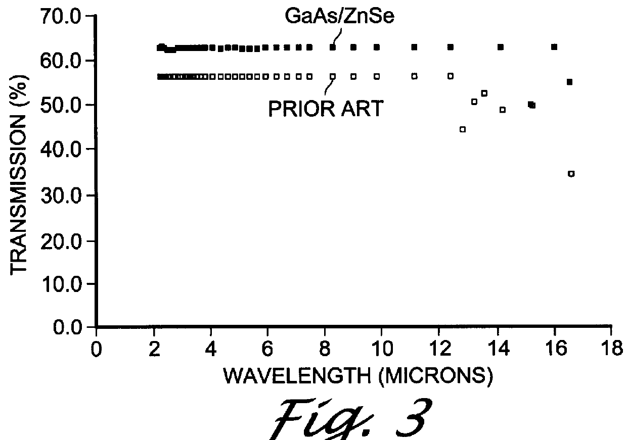
Layered over the doped conductive gallium arsenide layer 12 of Example 1 are a plurality of dielectric layers which are thermally evaporated on by techniques well known in the art to form an anti-reflection stack. These layers are formed of zinc sulfide, germanium and flouride compounds, and have thicknesses of the order of 0.3 microns. Similar dielectric layers are deposited on the bottom surface of the zinc selenide substrate 14. Inherent transmission of a window according to Example 2 is at least about 98.4% over the infrared spectrum.
Login to View More PUM
 Abstract
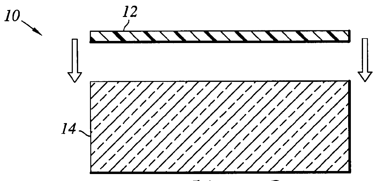
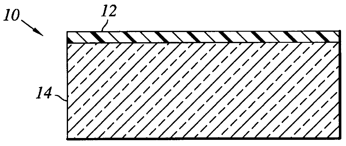
A semiconductor window which is transparent to light in the infrared range and which has good electrical conductivity is formed of a prefabricated semiconductor sheet bonded to a substrate material by optical contact. The sheet is a substantially uniformly doped wafer sufficiently thin that inherent absorption bands do not affect transmission. The sheet is contact bonded to the surface of an undoped transparent substrate without diffusion, growth or deposition on the surface. Windows having particular optical band pass characteristics are formed utilizing a zinc selenide substrate and a gallium arsenide sheet.
Description
The present invention relates generally to windows having an infrared transparent substrate and a transparent, electrically conductive semiconductor sheet laminated hereto.Transparent conductive windows through which optical energy must pass and which have good electrical conductivity have utility in a number of applications. These include resistance heated windows, electromagnetic interference (EMI) shielded windows, anti-static windows and transparent electrodes.In U.S. Pat. Nos. 4,778,731, 4,939,043, and 5,173,443, transparent conductive windows, coatings and methods of manufacture are described. In these patents the conductive component was either a thin coating applied by vacuum deposition techniques or a doped layer of semiconductor fabricated, in situ, into the structural window substrate made of the same semiconductor, or at least a compatible semiconductor.Windows fabricated utilizing a thin conductive coating applied by vacuum deposition require the use of substrate materi...
Claims
Login to View More Application Information
Patent Timeline
 IPC IPC(8): G02B5/20
CPCG02B5/207G02B5/208Y10T428/26
Inventor TULLY, JOHN W.MCCOY, DON L.SORENSEN, RICHARD F.
Owner NORTHROP GRUMMAN SYST CORP