Thin film semiconductor and method for manufacturing the same, semiconductor device and method for manufacturing the same

a technology of thin film semiconductor and manufacturing method, applied in the direction of semiconductor devices, electrical equipment, transistors, etc., can solve the problems of grain obstruction, high density of crystal nuclei, and unsatisfactory thin film transistors

Inactive Publication Date: 2000-10-17
SEMICON ENERGY LAB CO LTD
View PDF5 Cites 113 Cited by
  • Summary
  • Abstract
  • Description
  • Claims
  • Application Information

AI Technical Summary

Problems solved by technology

However, even if the technique mentioned above is employed in the active layer of a thin film transistor, the resulting thin film transistor is still unsatisfactory when used as a transistor constituting various types of arithmetic circuit, memory circuit, or the like, because the crystallinity thereof as an active layer is yet insufficient to suffice the required characteristics.
Thus, in the conventiona

Method used


Image

  • Thin film semiconductor and method for manufacturing the same, semiconductor device and method for manufacturing the same
  • Thin film semiconductor and method for manufacturing the same, semiconductor device and method for manufacturing the same
  • Thin film semiconductor and method for manufacturing the same, semiconductor device and method for manufacturing the same

Examples


embodiment 2

The present embodiment refers to a constitution similar to that described in Embodiment 1, except that the irradiation of a laser light is replaced by the same of an intense light having an energy equivalent to that of the laser light. RTA (rapid thermal annealing) is known as a technique for implementing the constitution of the present embodiment.

RTA is a method which comprises irradiating an intense light such as an infrared light or an ultraviolet light to the object by using a lamp, etc. The method is characterized in that the treatment can be completed in a short period of time of about several to several tens of seconds, and it can be conducted at a high heating and cooling rates. Thus, the thin film on the outermost surface alone can be heated. More specifically, for instance, only the thin film formed on the surface of a glass substrate can be annealed at an extremely high temperature of about 1,000.degree. C.

In this method, the throughput also can be considerably increased ...

embodiment 3

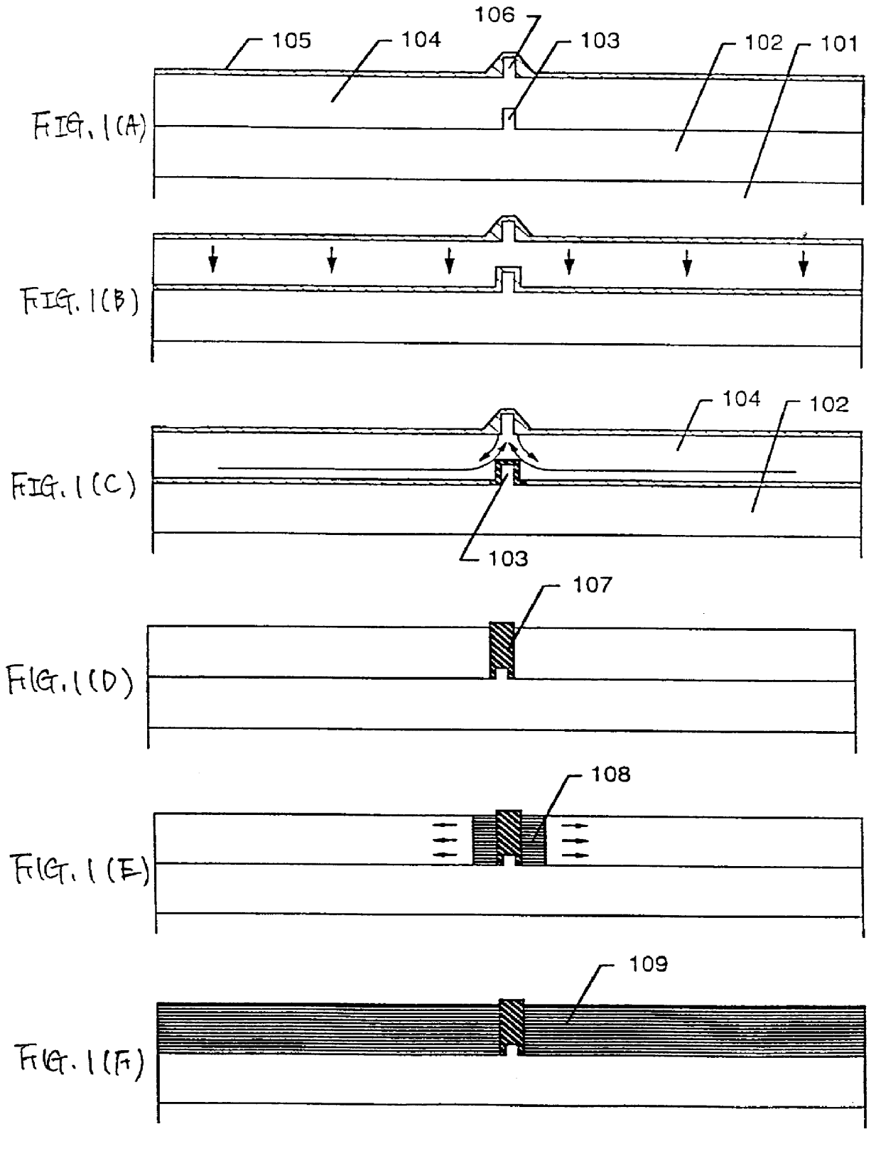
The present embodiment refers to a constitution in which an active layer of a thin film transistor is constructed by using a monodomain region obtained in the process steps described in Embodiment 1. Although a top gate type constitution is described in the present embodiment, it is also possible to apply the constitution to a bottom gate type.

Referring to FIG. 4(A), a thin film semiconductor comprising a monodomain region is formed in accordance with the process steps described in Embodiment 1, and is patterned to form an active layer 403 consisting of monodomain region alone. Similarly, as is described in Embodiment 1, reference numeral 401 is a glass substrate and reference numeral 402 is a silicon oxide film.

Then, a 1,500 .ANG. thick silicon oxide film 404 which functions as a gate insulating film is formed by plasma CVD. A silicon oxynitride film or a silicon nitride film may be used in the place of the silicon oxide film.

A 5,000-.ANG.-thick aluminum film 405 is formed by sputt...

embodiment 4

Recently, a structure comprising a single crystal formed on a silicon substrate having a silicon oxide film interposed therebetween, i.e., the so-called SOI structure, is attracting much attention. As a break through for a device of low energy consumption, the study on an SOI structure is in a rapid progress.

Substantially, the monodomain region according to the present invention has a crystallinity well equivalent to that of a single crystal. Accordingly, it can be readily applied to a SOI technique. In the present invention, problems yet to be solved for an SOI substrate is considered in comparison with the present invention.

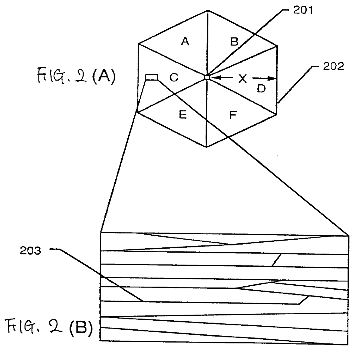
The problems remaining yet to be solved in the SOI technique are summarized in FIG. 5. Referring to FIG. 5, it can be seen that the problems include those related to crystallinity, such as the interface density level in the silicon film and fixed charges, and those attributed to external factors, such as metallic contamination and boron concentration.

In the pre...


PUM


Abstract

The present invention is related to a thin film semiconductor which can be regarded as substantially a single crystal and a semiconductor device comprising an active layer formed by the thin film semiconductor. At least a concave or convex pattern is formed intentionally on a insulating film provided in contact with the lower surface of an amorphous silicon film, whereby at least a site is formed in which a metal element for accelerating crystallization can be segregated. Therefore, a crystal nuclei is selectively formed in a portion where the concave or convex pattern is located, which carries out controlling a crystal diameter. Thus, a crystalline silicon film is obtained. A crystallinity of the crystalline silicon film is improved by the irradiation of a laser light or an intense light having an energy equivalent to that of the laser light, whereby a monodomain region in which no grain boundary substantially exit is formed.

Description

1. Field of the InventionThe present invention relates to a thin film semiconductor having a region which can be regarded as substantially a single crystal (hereinafter referred to as "a monodomain region"), and is formed on a substrate having an insulating surface, and to a semiconductor device using the thin film semiconductor as an active layer. More particularly, the present invention relates to a thin film transistor having an active layer constituted by a crystalline silicon film.2. Description of the Related ArtIn recent years, a technique for constituting a thin film transistor (TFT) by using a thin film silicon film (having a thickness of from several hundred to several thousand of angstroms (.ANG.)) formed on a substrate having an insulating surface has drawn a considerable attention. A thin film transistor is widely applied to electronic devices such as ICs and liquid crystal display devices.The most important portion of a thin film transistor is, so to speak the heart of...

Claims


Application Information

Patent Timeline
IPC IPC(8): H01L21/02H01L29/66H01L21/70H01L21/336H01L21/20H01L21/84H01L27/12H01L29/786H01L21/268H01L21/77
CPCH01L21/2022H01L27/12H01L29/66757H01L27/1281H01L29/78654H01L29/78675H01L27/1277H01L29/66772H01L21/02675H01L21/02672H01L21/0262H01L21/02532H01L21/02422H01L21/02669H10B10/125
Inventor YAMAZAKI, SHUNPEIMIYANAGA, AKIHARUKOYAMA, JUNFUKUNAGA, TAKESHI
Owner SEMICON ENERGY LAB CO LTD
Why Eureka
Try Eureka