

Organic electroluminescent device
a technology of electroluminescent devices and organs, applied in the direction of discharge tubes/lamp details, discharge tubes luminescnet screens, electric discharge lamps, etc., can solve the problems of low reliability of devices, easy oxidation, and lack of stability
- Summary
- Abstract
- Description
- Claims
- Application Information
AI Technical Summary
Benefits of technology
Problems solved by technology
Method used
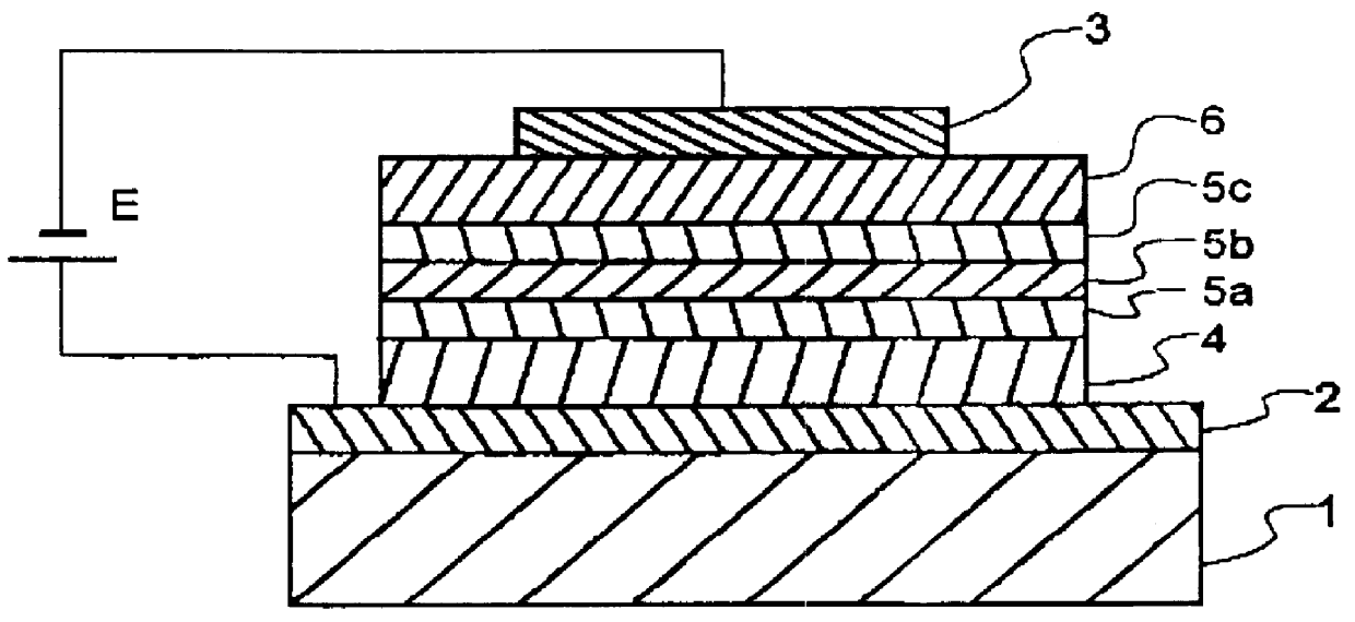
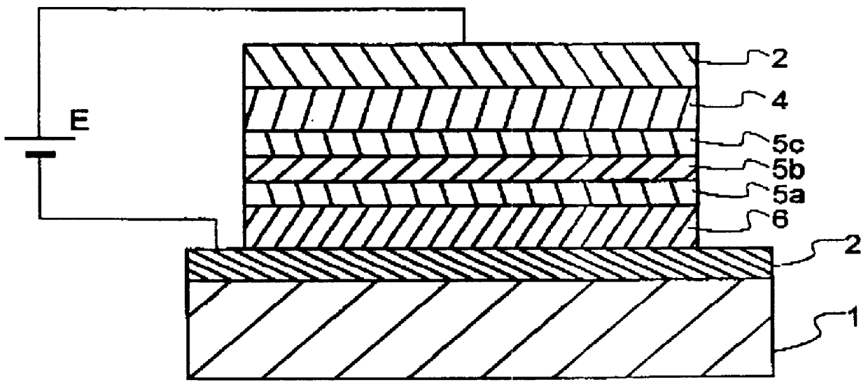
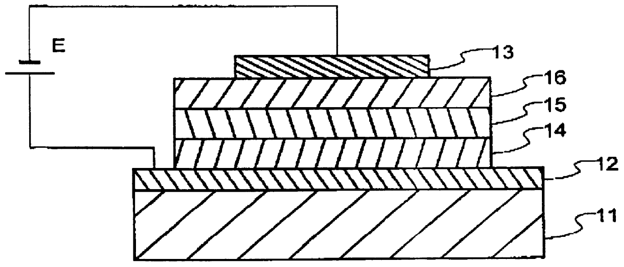
Image

Examples
example 1
A 7059 substrate (made by Corning) used as a glass substrate was scrubbed with neutral detergent. Then, the substrate was fixed to a substrate holder in a sputtering system, where an ITO hole injecting electrode layer was formed by a DC magnetron sputtering process using an ITO oxide target.
The substrate with the ITO film formed on it was ultrasonically washed with neutral detergent, acetone, and ethanol, and then pulled up from boiling ethanol, followed by drying. The substrate was subsequently cleaned on its surface with UV / O.sub.3. Then, the substrate was fixed to the substrate holder in the sputtering system, which was evacuated to a vacuum of 1.times.10.sup.-4 Pa or lower.
Then, a 1-nm thick inorganic insulating hole injecting and transporting layer was formed using SiO.sub.2 for a target. The sputtering gas used comprised Ar mixed with 5% of O.sub.2. The substrate temperature, film formation rate, operating pressure, and input power were 25.degree. C., 1 nm / min., 0.5 Pa, and 5 ...
example 2
Experiments were carried out as in Example 1 with the exception that the main component and stabilizer in the inorganic insulating electron injecting and transporting layer were changed from SrO to MgO, CaO or an oxide mixture thereof, from Li.sub.2 O to K.sub.2 O, Rb.sub.2 O, K.sub.2 O, Na.sub.2 O, Cs.sub.2 O or an oxide mixture thereof, and from SiO.sub.2 to GeO.sub.2 or an SiO.sub.2 and GeO.sub.2 oxide mixture. The obtained results were much the same as Example 1. The same was also true of when the cathode constituting material was changed from Al to Ag, In, Ti, Cu, Au, Mo, W, Pt, Pd, Ni or an alloy thereof.
example 3
An organic EL device was prepared and estimated for life performance as in Example 1 with the exception that an inorganic insulating hole injecting and transporting layer having a composition of SiO.sub.1.9 was formed using a target having a composition of SiO.sub.2 and varying the flow rate of O.sub.2 in the sputtering gas to an O.sub.2 to Ar mixing ratio of 5%. The obtained results were much the same as Example 1.
Organic EL devices were prepared and estimated as in Example 1 with the exception that a layer having an SiO.sub.1.95 composition was formed using a target having an SiO.sub.2 composition and varying the flow rate of O.sub.2 in the sputtering gas to an O.sub.2 to Ar mixing ratio of 30%, a layer having a GeO.sub.1.96 composition was formed using a target having a GeO.sub.2 composition and varying the flow rate of O.sub.2 in the sputtering gas to an O.sub.2 to Ar mixing ratio of 30%, and a layer having an Si.sub.0.5 Ge.sub.0.5 O.sub.1.92 composition was formed using a targe...
PUM
 Abstract
Description
Claims
Application Information