Control of size and heat affected zone for fine pitch wire bonding

a fine pitch wire bonding and control technology, applied in the field of wire bonding, can solve the problems of inability to tolerate soldering or welding, slow process, and substantial temperature excursions in the process, and achieve the effect of economic impracticality, and reducing the cost of production

Inactive Publication Date: 2001-01-30
IBM CORP
View PDF18 Cites 110 Cited by
  • Summary
  • Abstract
  • Description
  • Claims
  • Application Information

AI Technical Summary

Problems solved by technology

At the current state of the art, however, many applications in which wire bonding is needed cannot tolerate either soldering or welding because of the size of the resulting bond or the heat budget of the device to which a connection must be made.
While thermal compression bonding produces high quality bonds, the process involves substantial temperature excursions and is slow; becoming economically impractical as the number of required wire bonds increases.
However, wire bonds formed by this technique are directional in that the axis of the wire is "wedged" parallel to the pad surface and obtaining the correct wire orientation in the plane of the pad surface is difficult and may require complex automated manipulations, including rotation of a mandrel-like transducer by which ultrasonic energy is applied and across which the wire is fed, which may slow the process significantly.
The heat of the arc (and any resistive heating which may occur) is difficult to regulate from one free air ball formation to the next and therefore ball size will unavoidably vary within and beyond the range indicated above.
Further a threshold amount of energy will be required to reliably strike an arc to form the free air ball and this threshold cannot be scaled with wire diameter.
Therefore, average minimum size as well as the variability of size of the free air ball may increase with decreasing wire size and, in any event, is uncontrolled.
Further, annealing may cause the grain size to approach 1 mil which infers that a few grain boundaries may cover a significant portion of the cross-sectional area of a 1.25 mil wire within the HAZ and potentially the entire cross-section of the wire if wire diameter is reduced.
It can thus be understood that annealing can also cause substantial weakening of fine wires which could then be broken by relatively small tensile forces which can occur during subsequent assembly processes.
Thus the geometry of the wire routing is less readily controllable both during formation of the connection and thereafter until the wire bond is encapsulated to complete the packaging of the electronic device.
Since connections formed by wire bonding may cross and wire bonds may be formed closely adjacent each other, any of these deformations, alone or in any combination may potentially cause shorting between wires of respective connections.
Insulation cannot be provided on the wire without contamination of the bonding surfaces.
Therefore, wire bond connections may become shorted together as formed and are subject to damage due to even relatively slight accelerations or inadvertent contact with other structures before encapsulation can be performed or even due to viscous drag of applied materials during the encapsulation process itself.
However, such a tall loop configuration actually increases the likelihood of shorting as wire bond connections are made closer together.
Moreover, a greater height of encapsulation may compromise other processes such as package heat dissipation, post-assembly cleaning, solder connection pitch or second level attachment processes such as ball grid array (BGA) techniques.
Nevertheless, the functionality of any chip is limited by the capacity for conducting signals to it or away from it.
Therefore, the potential for reduction of chip area is often limited by the area occupied by connection pads and wire bonding pads in particular.
However, even for smaller reductions in wire bond pitch (e.g. to less than 90 microns) it is evident that more stringent tolerances will be required for free air ball diameter than can presently be produced by known techniques and that smaller diameter wire will be required which will increase the difficulty of obtaining uniform and reduced dimensions of free air balls.
Reduced wire size will also tend to increase the size of the heat affected zone in the wire while making the malleability and weakness of the wire substantially more critical to manufacturing yield.
Nevertheless, the functionality of chips which can be developed at the present and foreseeable state of the art will require wire bond pitches of 60 microns or less at which the size and uniformity of free air ball diameter and extent of the HAZ will be extremely critical and beyond the capability of current techniques notwithstanding the fact that significantly smaller wire diameter will be required.

Method used


Image

  • Control of size and heat affected zone for fine pitch wire bonding
  • Control of size and heat affected zone for fine pitch wire bonding
  • Control of size and heat affected zone for fine pitch wire bonding

Examples


Embodiment Construction

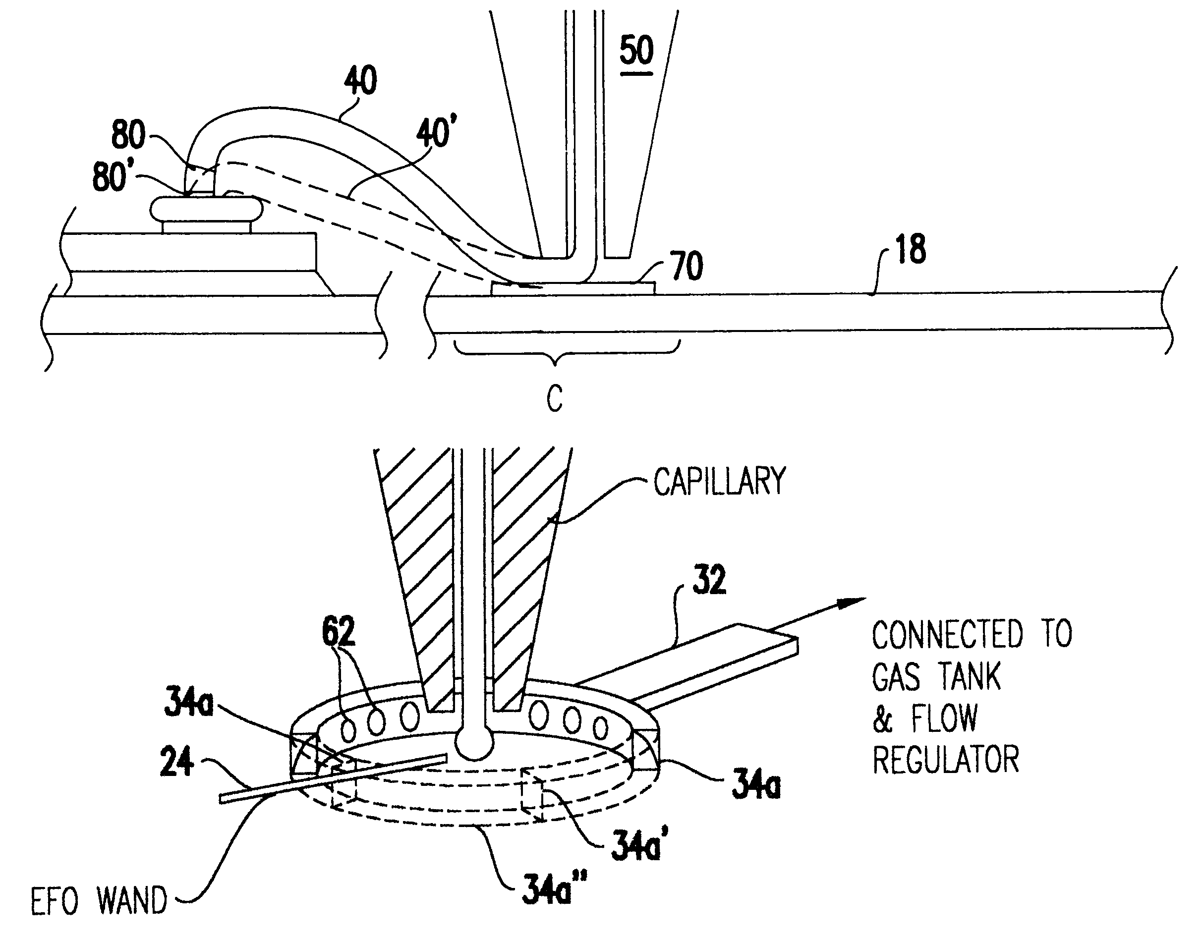
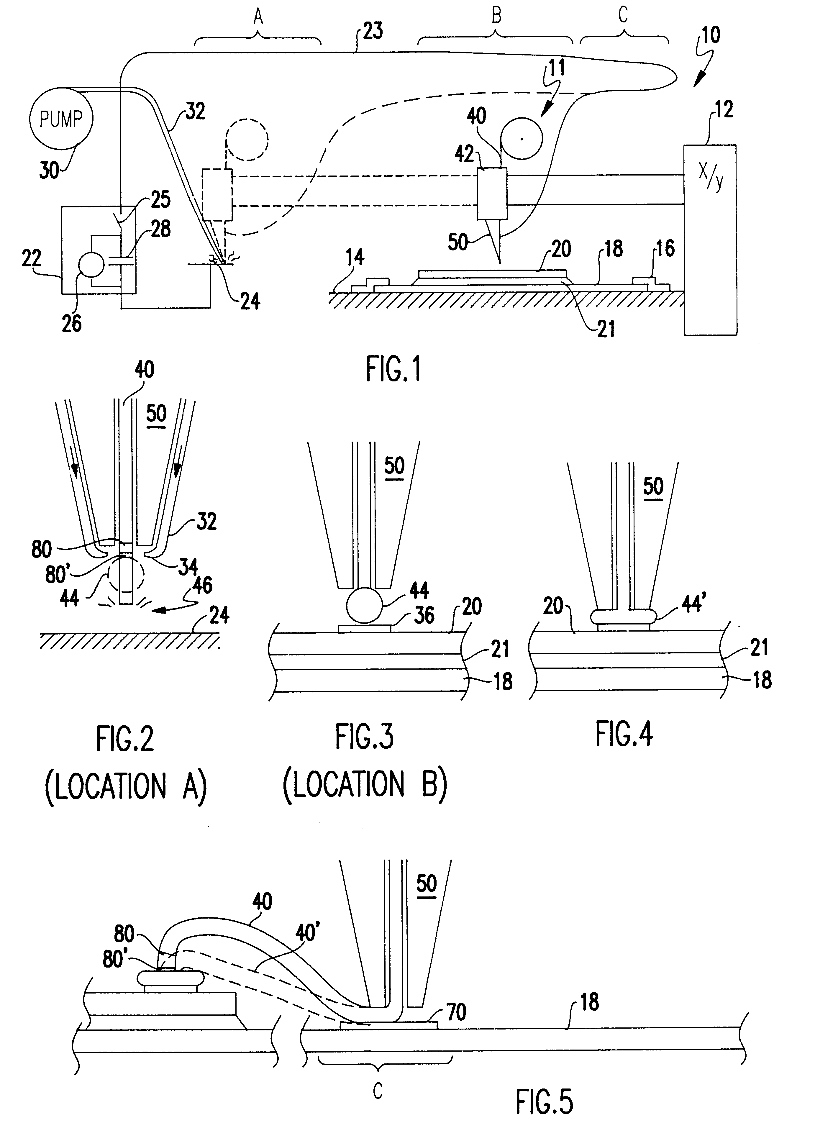
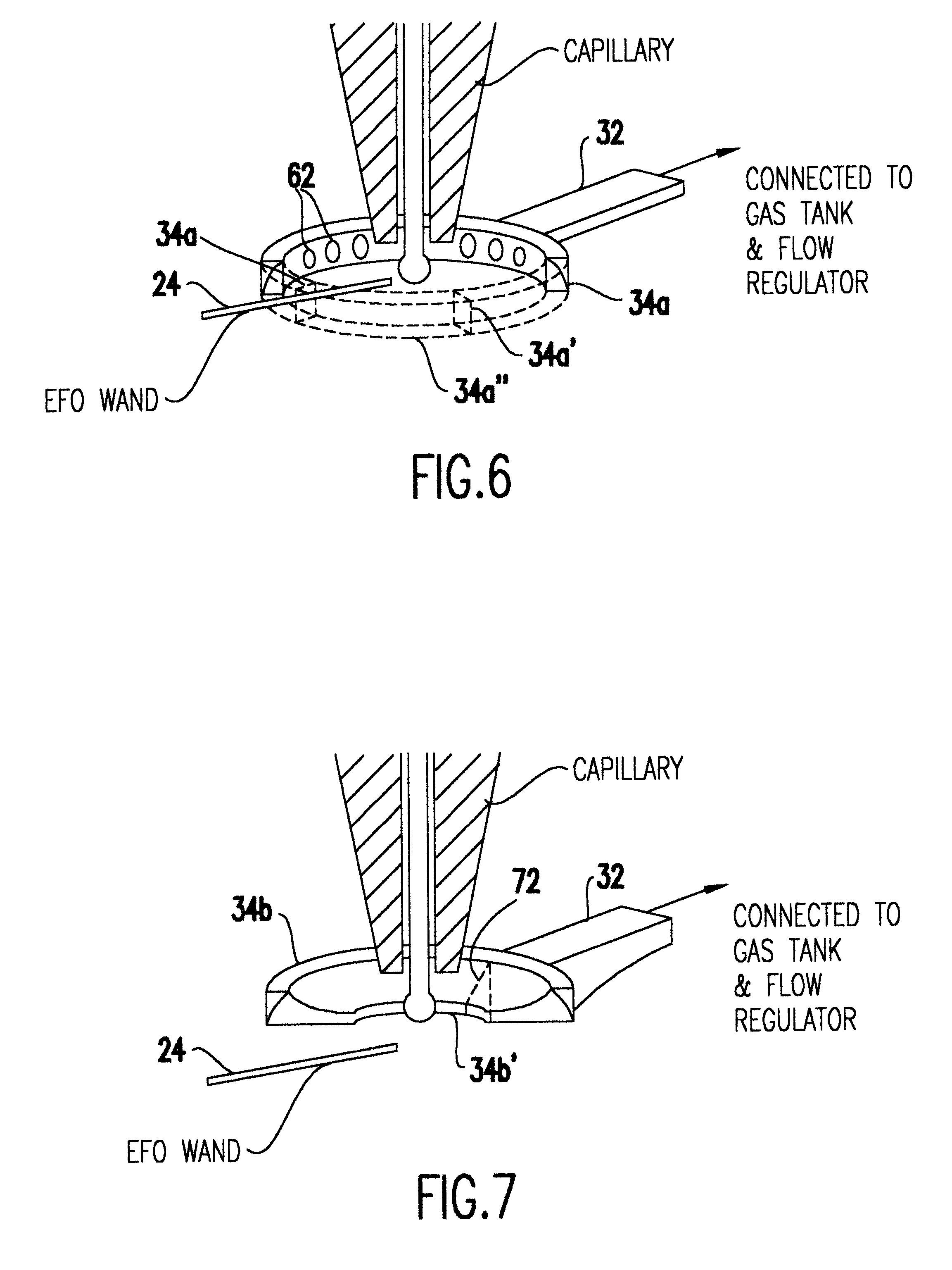
Referring now to the drawings, and more particularly to FIG. 1, there is schematically shown an apparatus 10 for performing thermosonic bonding in accordance with the invention, particular steps of which are illustrated in enlarged form in FIGS. 2-5. It is to be understood that wire bonding is generally done with gold wire which is to be bonded to gold pads. In such a case, since gold does not oxidize, no enclosure for providing any particular atmosphere is required and none is shown in FIG. 1 in the interest of clarity. If other materials such as copper or aluminum are to be bonded, it is preferred to carry out wire bonding in an oxygen-free atmosphere such as nitrogen or argon gas and to provide a suitable enclosure to contain the gas. For example, since argon gas is heavier than air, a simple barrier to form a cup-shaped enclosure is adequate.

The apparatus 10 includes a bonding head 11, a transport mechanism 12 for moving the head relative to a conductive structure 24 at location...


PUM

PropertyMeasurementUnit
thicknessaaaaaaaaaa
diameteraaaaaaaaaa
diameteraaaaaaaaaa

Abstract

The amount of melting of the bonding wire is closely regulated, and reduction of size and improvement of uniformity of the free air ball is obtained for ball bonding at pitches of less than ninety mils even when bonding wire of reduced diameter is employed. Quenching of the bonding wire adjacent to the free air ball also limits the temperature rise in the bonding wire and the extent of a heat affected zone having less tensile strength and stiffness to less than one micron and with reduced grain enlargement. The present invention provides such a bond for electronic packaging of increased reliability, potential functionality, increased manufacturing yield and reduced process complexity.

Description

1. Field of the InventionThe present invention generally relates to wire bonding for a manufacturing process and, more particularly, ball wire bonding suitable for forming wire bonds at a fine pitch to integrated chips and package structures for fabrication of electronic devices.2. Description of the Prior ArtMiniaturization of electronic devices provides not only manufacturing economies but provides performance enhancement by reducing signal propagation time between nodes of the electronic device. At the high performance levels which currently characterize modern digital circuits, design rules provide for extremely close spacing of components and connections therebetween. The vast majority of connections are therefore made on integrated circuit chips by lithographic processes as part of the integrated circuit design. However, many connections to integrated circuit chips are made by wire bonding. It is also possible, in view of the complexity and cost of manufacture of integrated ci...

Claims


Application Information

Patent Timeline
Patent Type & Authority Patents(United States)
IPC IPC(8): B23K20/00H01L21/02H01L21/607
CPCB23K20/005H01L24/78H01L24/85B23K2201/40H01L24/45H01L2224/05644H01L2224/45015H01L2224/45124H01L2224/45144H01L2224/45147H01L2224/48091H01L2224/48227H01L2224/48465H01L2224/4851H01L2224/78302H01L2224/78313H01L2224/85045H01L2224/85075H01L2224/85205H01L2924/01006H01L2924/01007H01L2924/01013H01L2924/01018H01L2924/01029H01L2924/01079H01L2924/01082H01L2924/14H01L2924/19041H01L2924/20752H01L2924/00014H01L2224/48699H01L2224/73265H01L2224/85181H01L2224/92247H01L2924/01005H01L2924/01033H01L2924/014H01L2924/00H01L2924/00012H01L2224/48644H01L2224/48844H01L2224/48744H01L2224/48511H01L24/48B23K2101/40H01L2924/20753
Inventor MURDESHWAR, NIKHIL M.
Owner IBM CORP
Why Eureka
Try Eureka