Phase mask for manufacturing diffraction grating, and method of manufacture

a technology of diffraction grating and phase mask, which is applied in the field of diffraction gratingforming phase mask, can solve the problems of high manufacturing cost, low yield, and difficulty in making such a minute structure in the optical fiber cor

Inactive Publication Date: 2001-03-13
DAI NIPPON PRINTING CO LTD
View PDF14 Cites 40 Cited by
  • Summary
  • Abstract
  • Description
  • Claims
  • Application Information

AI Technical Summary

Problems solved by technology

At the beginning, it was considered difficult to make such a minute structure in an optical fiber core; that is, a Bragg diffraction grating was provided in the optical fiber core by a sophisticated process comprising a number of steps, e.g., side polishing, photoresist coating, holographic exposure, and reactive ion beam etching.
For this reason, much fabrication time was needed, resulting in low yields.
Regarding the two-beam interference process, a problem arises in conjunction with the quality of the b

Method used


Image

  • Phase mask for manufacturing diffraction grating, and method of manufacture
  • Phase mask for manufacturing diffraction grating, and method of manufacture
  • Phase mask for manufacturing diffraction grating, and method of manufacture

Examples


example 1

FIG. 5(a) to FIG. 5(h) are sectional views of one embodiment of the process of fabricating the aforesaid phase mask 1. In these figures, reference numeral 5 represents a phase mask blank, 2 a quartz substrate, 4 a chromium thin film, 4A a chromium thin-film pattern, 4B an opening in the chromium thin film, 6 an electron-beam resist, 6A a resist pattern, 6B a resist opening, 14 an electron beam, 1 a phase mask, 3 a groove of a sine wave shape in section, 3' a groove of a rectangular wave shape in section, 8 a strip of a sine wave shape in section, and 8' a strip of a rectangular wave shape in section.

As shown in FIG. 5(a), the blank 5 was first prepared by forming the chromium thin film 4 of 20 nm in thickness on the quartz substrate 2 by sputtering. The chromium thin film 4 is useful for preventing a charging-up of the electron-beam resist 6 at the electron-beam (6) irradiation step, and serves as a mask in the formation of the groove 3' on the quartz substrate. The thickness of thi...

example 2

In this example, steps (a) to (b) are the same as those shown in FIGS. 5(a) to 5(d) for Example 1. That is, the blank 5 was first prepared by forming the chromium thin film 4 of 20 nm in thickness on the quartz substrate 2 by sputtering, as shown in FIG. 5(a).

Then, electron-beam resist RE5100P (made by Hitachi Kasei Co., Ltd.) as the electron-beam resist 6 was coated on the chromium thin film to a thickness of 400 nm, and dried, as shown in FIG. 5(b).

After this, the electron-beam resist 6 was exposed to light at an exposure of 1.2 .mu.C / cm.sup.2, as shown in FIG. 5(c), using an electron-beam writing system MEBESIII (made by ETEC), so that portions corresponding to the groove 3' were exposed to the electron beams 7.

After the exposure, post-exposure baking (PEB) was carried out at 90.degree. C. for 5 minutes, and the electron-beam resist 6 was developed with TMAH (tetramethylammonium hydroxide) at a concentration of 2.38%, thereby forming such desired resist pattern 6A as shown in FIG...

example 3

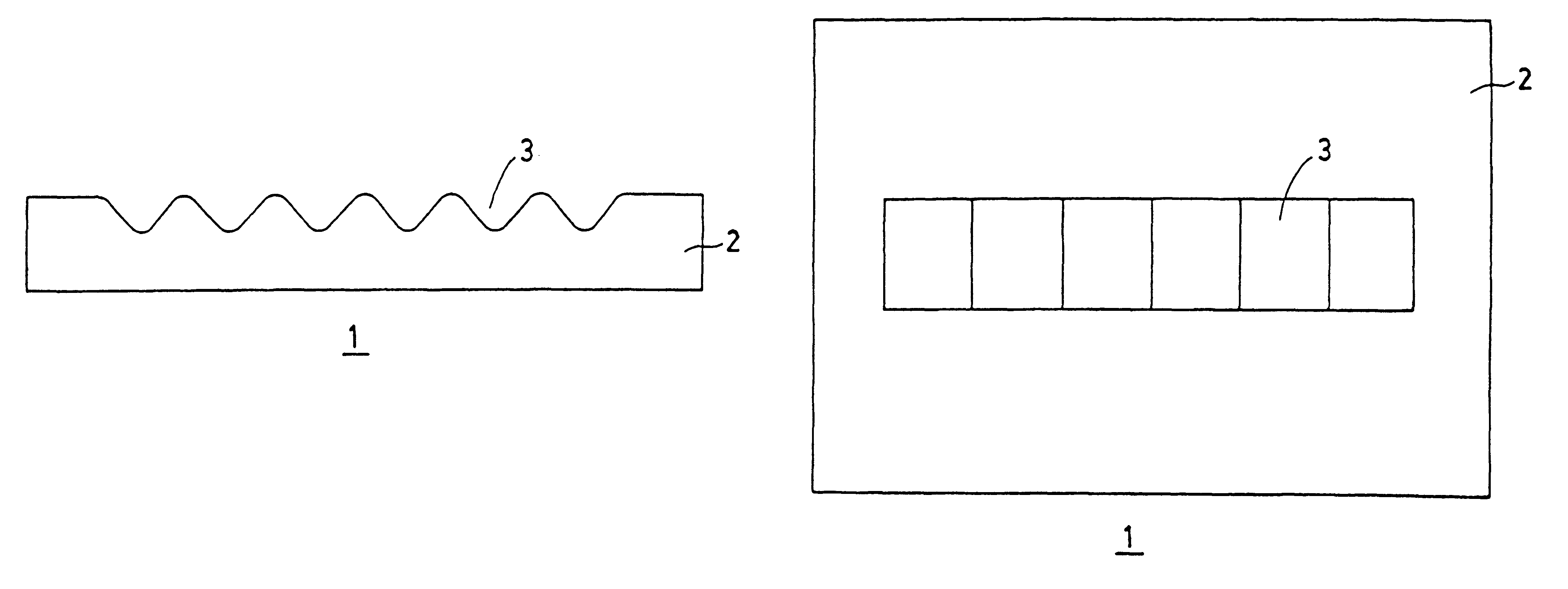
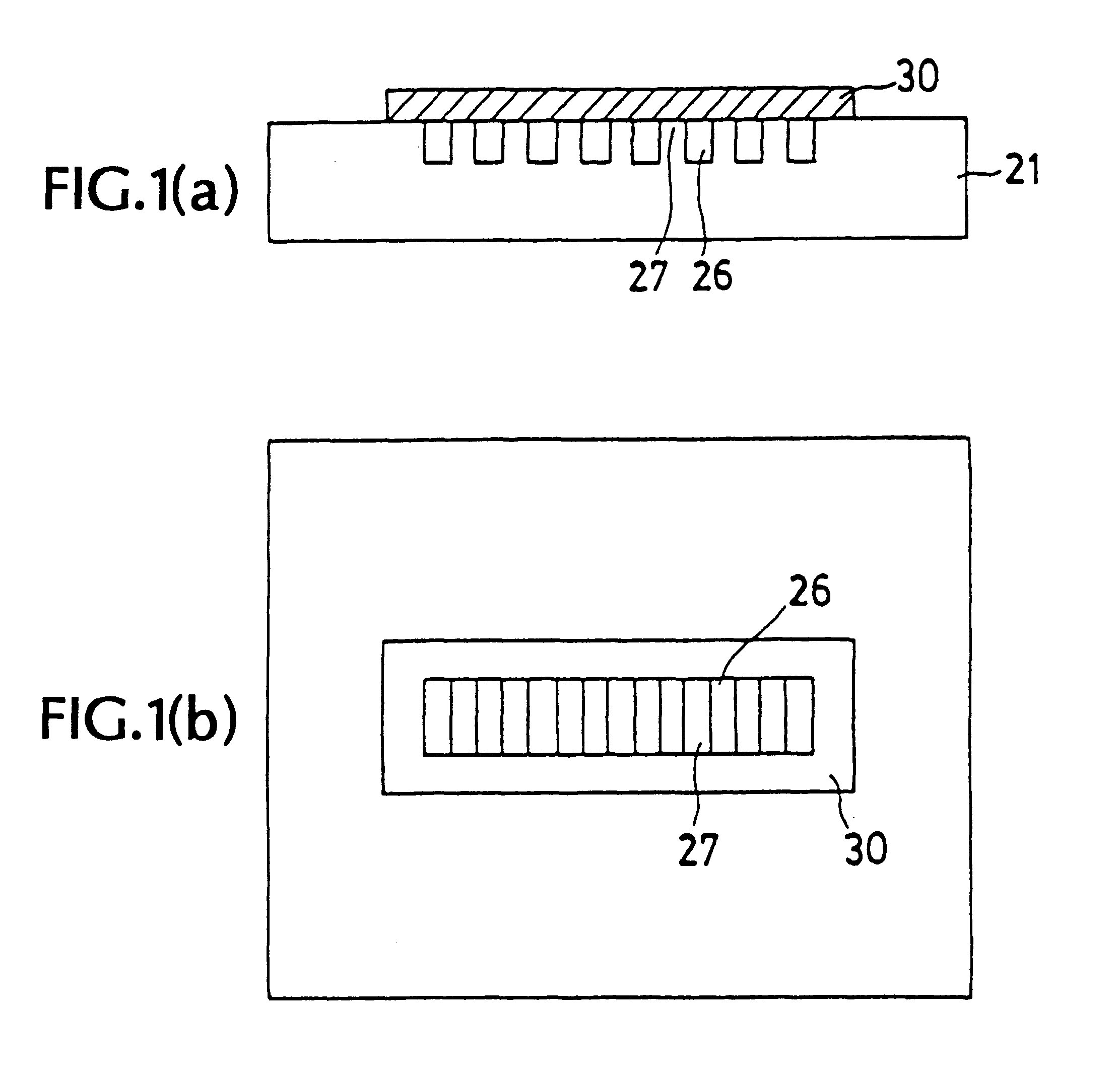
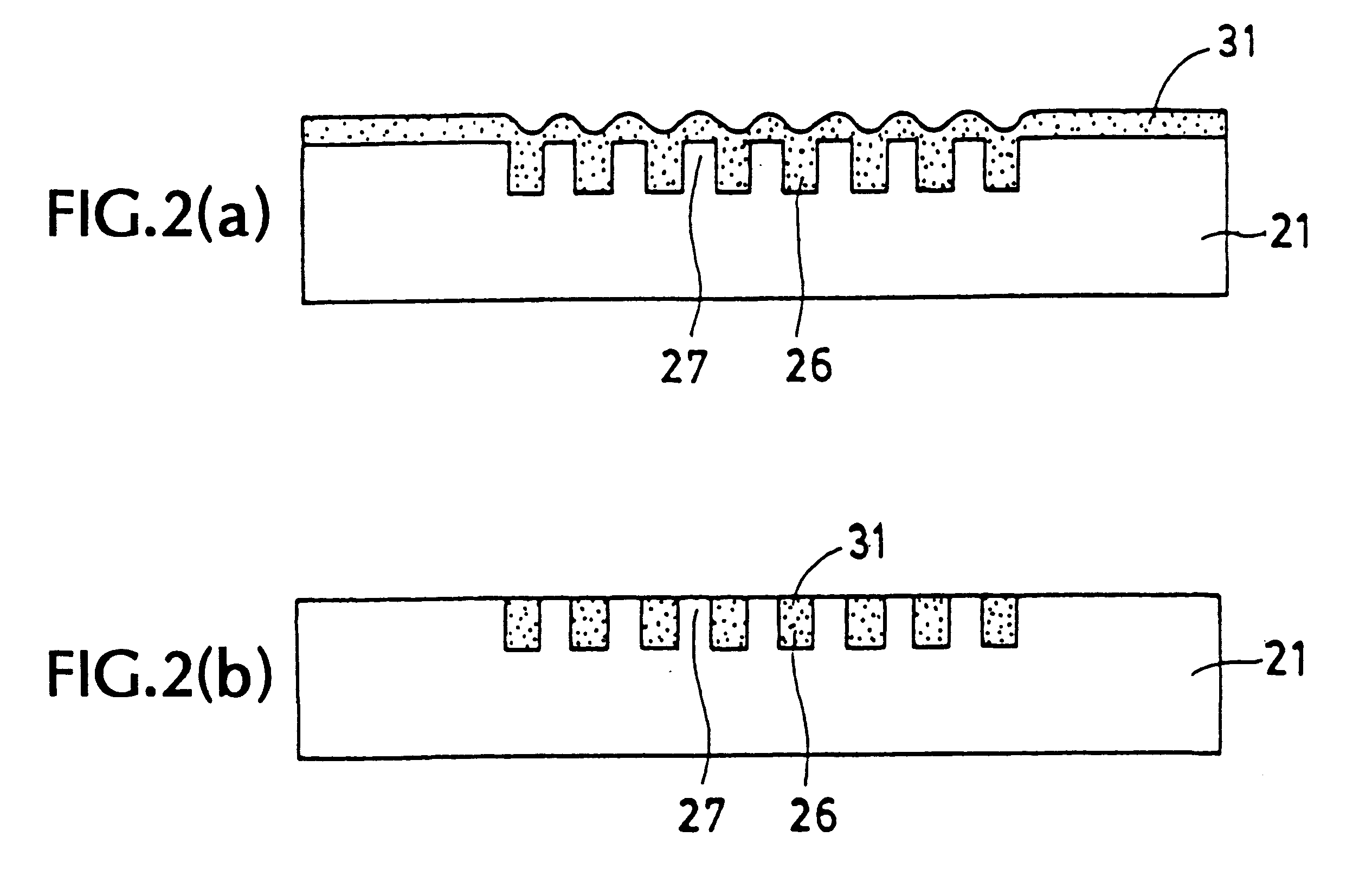
Using the method as already explained, a transparent protective layer 30 was applied over the surface of the transparent substrate (FIG. 1) fabricated according to the FIG. 5 or 6 fabrication process. The section of the repetitive groove (26)-and-strip (27) pattern shown in FIG. 1 was in a substantially sine wave shape, as can be seen from the phase mask fabricated according to the FIG. 5 or 6 fabrication method. The transparent protective layer 30 was applied with respect to this phase mask, thereby covering the surface of the transparent substrate shown in FIG. 1.


PUM


Abstract

The invention relates to a diffraction grating-forming phase mask which can make the diffraction grating to be formed substantially free of any defect, even when foreign matters or resins, etc. sublimed from an optical fiber are deposited on the surface of the phase mask. The phase mask 21 comprises a substrate and a grating form of repetitive groove (26)-and-strip (27) pattern for forming a diffraction grating by interference fringes of diffracted light through the repetitive pattern. An optically transparent protective layer 30 is applied over the surface of the substrate with the repetitive groove (26)-and-strip (27) pattern formed thereon.

Description

TECHNICAL ARTThe present invention relates generally to a diffraction grating-forming phase mask and its fabrication method, and more particularly to a phase shift mask for using ultraviolet laser light to form a diffraction grating in an optical fiber used for optical communications, etc.Optical fibers have brought about breakthroughs in the globalization of communications to make high-quality and large-capacity inter-oceanic telecommunications feasible. So far, it has been known that a Bragg diffraction grating is provided in an optical fiber by creating a periodic refractive index profile in an optical fiber core along the optical fiber, and the magnitude of reflectivity and the width of the wavelength characteristics of the diffraction grating are determined by the period and length and the magnitude of refractive index modulation of the diffraction grating, whereby the diffraction grating can be used as a wavelength division multiplexer for optical communications, a narrow-band...

Claims


Application Information

Patent Timeline
IPC IPC(8): G02B5/18G03F1/00
CPCG02B5/1857G02B6/02138G03F1/34
Inventor KURIHARA, MASAAKISEGAWA, TOSHIKAZU
Owner DAI NIPPON PRINTING CO LTD
Why Eureka
Try Eureka