Package for semiconductor power device and method for assembling the same

Inactive Publication Date: 2001-03-13
KK TOSHIBA
View PDF8 Cites 139 Cited by
  • Summary
  • Abstract
  • Description
  • Claims
  • Application Information

AI Technical Summary

Problems solved by technology

However, the above-described conventional IPM has several technical problems that are derived from the structure thereof.
However, it is impossible to remove the generation of the openings and joints completely, leaving a tiny opening or joint within the semiconductor device.
In addition, bonding the components strongly may increase the heat stress in a portion where different thermal expansion coefficients exist between components such as the outer case 6 and the heat sink (conductive bottom plate) 5, and may cause a breakage of the outer case 6 and an enlargement of the opening remained.
The breakage of the outer case 6 and the enlargement of the opening may invite a moisture absorption by the silicone gel, resulting in a cause to degrade electrical properties and durability thereof.
Second, adding a component such as the pressure-releasing valve for relieving the heat stress inside the IPM may complicate an inner structure of the device and increase a size of the entire device.
Third, since the conventional IPM is produced from several materials such as the outer case 6, the lid (terminal holder) 8, the silicone gel 91 and the epoxy resin, the heat stress may be generated due to the differences among the thermal expansion coefficients of the materials, and a complicated

Method used


Image

  • Package for semiconductor power device and method for assembling the same
  • Package for semiconductor power device and method for assembling the same
  • Package for semiconductor power device and method for assembling the same

Examples


first embodiment

The first embodiment shown in FIGS. 2A-4B may be combined with the second embodiment. Combined structures that apply the smooth region 2a shown in FIG. 5 to the structures having the solidified insulating material, or the resin 11 shown in FIG. 4A, the thick resin 12 shown in FIG. 4A and the resin 11 with the heaped member 13 shown in FIG. 4B are desirable. According to these structures, both the advantages from the first and second embodiments are obtained at the same time. Coating the resins 11 and 12 over the smooth region 2a may increase the adhesion among the resins 11, 12 and the AlN substrate 2 and the improvement of the reliability to be expected.

second embodiment

MODIFICATION OF

To further relax the electric field strength, the solidified insulating material, or the hardened epoxy resin can be provided on the edges of the semiconductor power chips 21, 23 and the control circuitry chip 22 in the structure of the second embodiment or in the structure in combination of the second and first embodiments. If the epoxy resin that has the intermediate dielectric constant between those of the AlN substrate 2 and the silicone gel 91 is coated on the edges of the semiconductor power chips 21 and 23, the electric field at the edge of the top copper film 1a can be relaxed. Containing the powdered Al.sub.2 O.sub.3 (dielectric constant: about 8.3) in the resins 11-13 may further relax the electric filed and prevent the creeping discharge. The AlN powders may be filled instead of the Al.sub.2 O.sub.3. Both the Al.sub.2 O.sub.3 and AlN powders may also be filled together.

third embodiment

(THIRD EMBODIMENT)

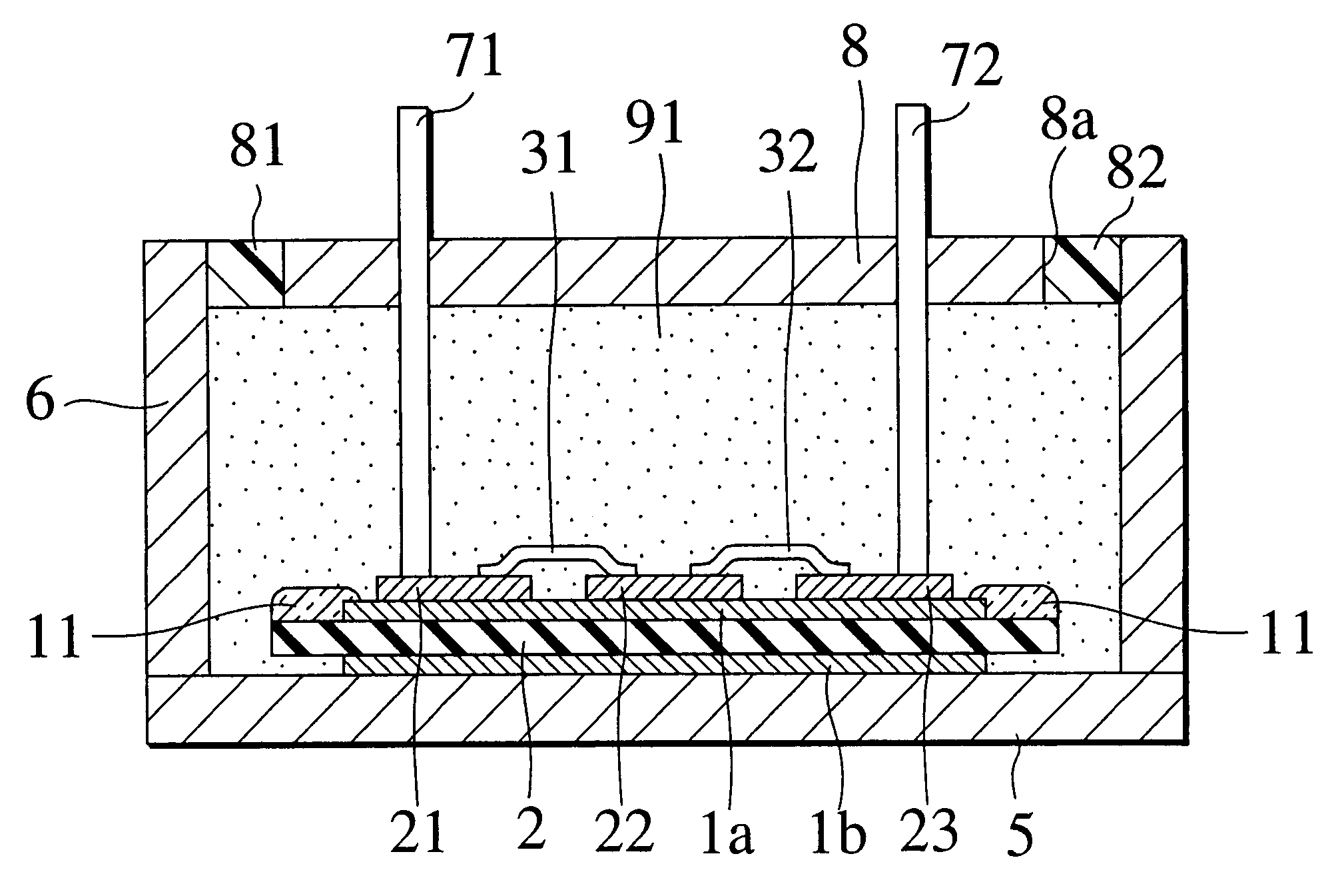
FIG. 6 is a cross sectional view showing a structure of a package for semiconductor power device according to a third embodiment of the present invention. The third embodiment adopts a structure that has a polished smooth region 2b at a bottom surface of an AlN substrate 2, which faces to a conductive bottom plate 5 serving as a heat sink and also opposes to an exposed top surface of a peripheral region of the AlN substrate 2 as shown in FIG. 6, instead of the smooth region 2a at the exposed top surface of the AlN substrate 2 in the second embodiment.

Similar to the second embodiment, the package for a semiconductor power device according to the third embodiment of the present invention employs the AlN substrate 2 that includes a top copper film 1a and a bottom copper film 1b disposed on a top and under a bottom surfaces of the AlN substrate 2, respectively, except the peripheral region by the DBC technique as same as the first embodiment. The top copper film 1a on ...


PUM


Abstract

A package for a semiconductor power device which comprises: a conductive bottom plate as a heat sink; an insulating substrate mounted on the bottom plate; a copper film formed on the insulating substrate to expose a peripheral region of the insulating substrate; semiconductor chips disposed on the copper film; a container arranged on the bottom plate, surrounding the insulating substrate; an external terminal supported through the container and connected electrically with the semiconductor chips; and a silicone gel filled within the container, wherein a solidified insulating material is disposed on an outer edge region of the copper film and the peripheral region of the insulating substrate. Thus, reducing an electric field across the interface and making it difficult to cause a creeping discharge. A notch is formed in the bottom plate, and the notch is filled with a high heat conductive resin. The notch is located outwardly apart from a region where the semiconductor chips are mounted. Thus, a creeping breakdown is prevented without sacrificing a heat radiation effect of the bottom plate. Using a waterproof and flexible film to seal an inlet for filling the silicone gel into the case, a heat stress caused by an expansion and a shrinkage of the silicone gel in response to a variation of temperatures is reduced, and it prevents the silicone gel from being wet. A thermoplastic insulating resin is employed instead of the silicone gel.

Description

1. Field of the InventionThe present invention relates to a technology for increasing a breakdown voltage and reliability of a semiconductor power device, and more particularly to a packaging technology for preventing a dielectric breakdown of a power device module which has a plural of power switching devices mounted thereon and for increasing a breakdown voltage and reliability thereof.2. Description of the Related ArtSemiconductor power devices for converting and controlling the flow of electric energy have been greatly researched and developed in recent years in response to high requirements from various fields including the power electronics field at first. It is particularly required to realize a power switching device, for example, a Power MOSFET, a Power Bipolar Transistor (Power BJT), a Gate Turn-off (GTO) Thyristor and an Insulated Gate Bipolar Transistor (IGBT) that can control a high power and achieve a high performance. As the result, a high voltage semiconductor power ...

Claims


Application Information

Patent Timeline
IPC IPC(8): H01L23/16H01L23/31H01L23/34H01L23/433H01L23/24H01L23/28
CPCH01L23/24H01L23/3135H01L23/4334H01L24/48H01L24/49H01L23/3121H01L2924/1305H01L24/45H01L2224/45124H01L2224/45144H01L2224/45147H01L2224/48091H01L2224/48095H01L2224/48137H01L2224/48139H01L2224/48227H01L2224/48472H01L2224/48599H01L2224/48699H01L2224/49111H01L2924/01004H01L2924/01005H01L2924/01006H01L2924/01013H01L2924/01014H01L2924/01015H01L2924/01028H01L2924/01029H01L2924/01033H01L2924/01042H01L2924/01057H01L2924/01078H01L2924/01079H01L2924/01082H01L2924/01083H01L2924/014H01L2924/13055H01L2924/13091H01L2924/14H01L2924/19041H01L2924/1301H01L2924/01023H01L2924/0102H01L2924/00014H01L2924/00H01L2924/00012H01L2924/351H01L2924/15787H01L2224/45014H01L2924/181H01L2224/85399H01L2224/05599H01L2924/206H01L23/28
Inventor SHIMIZU, TOSHIOHIRAMOTO, HIROYUKISEKIYA, HIROKIKIGIMA, KENJI
Owner KK TOSHIBA
Why Eureka
Try Eureka