Method of forming reliable copper interconnects

Inactive Publication Date: 2001-04-03
GLOBALFOUNDRIES INC
View PDF3 Cites 58 Cited by
  • Summary
  • Abstract
  • Description
  • Claims
  • Application Information

AI Technical Summary

Problems solved by technology

Such escalating requirements have been found difficult to satisfy in terms of providing a low RC (resistance capacitance) interconnect pattern, particularly wherein submicron vias, contacts and trenches have high aspect ratios imposed by miniaturization.
Thus, the interconnection pattern limits the speed of the integrated circuit.
As integration density increases and feature size decreases in accordance with submicron design rules, the rejection rate due to integrated circuit speed delays approaches and even exceeds 20%.
However, as the size of openings for vias/contacts and trenches is scaled down to the sub-micron range, step coverage problems have arisen involving the use of Al which has decreased the reliability of interconnections formed between different wiring layers.
Such poor step coverage results in high current density and enhanced electromigration.
Moreover, low dielectric constant polyamide materials, when employed as dielectric interlayers, create moisture/bias reliability problems when in contact with Al.
For example, most W processes are complex and expensive.
Furthermore, W plugs are susceptible to void formation and the inter

Method used


Image

  • Method of forming reliable copper interconnects
  • Method of forming reliable copper interconnects
  • Method of forming reliable copper interconnects

Examples


Embodiment Construction

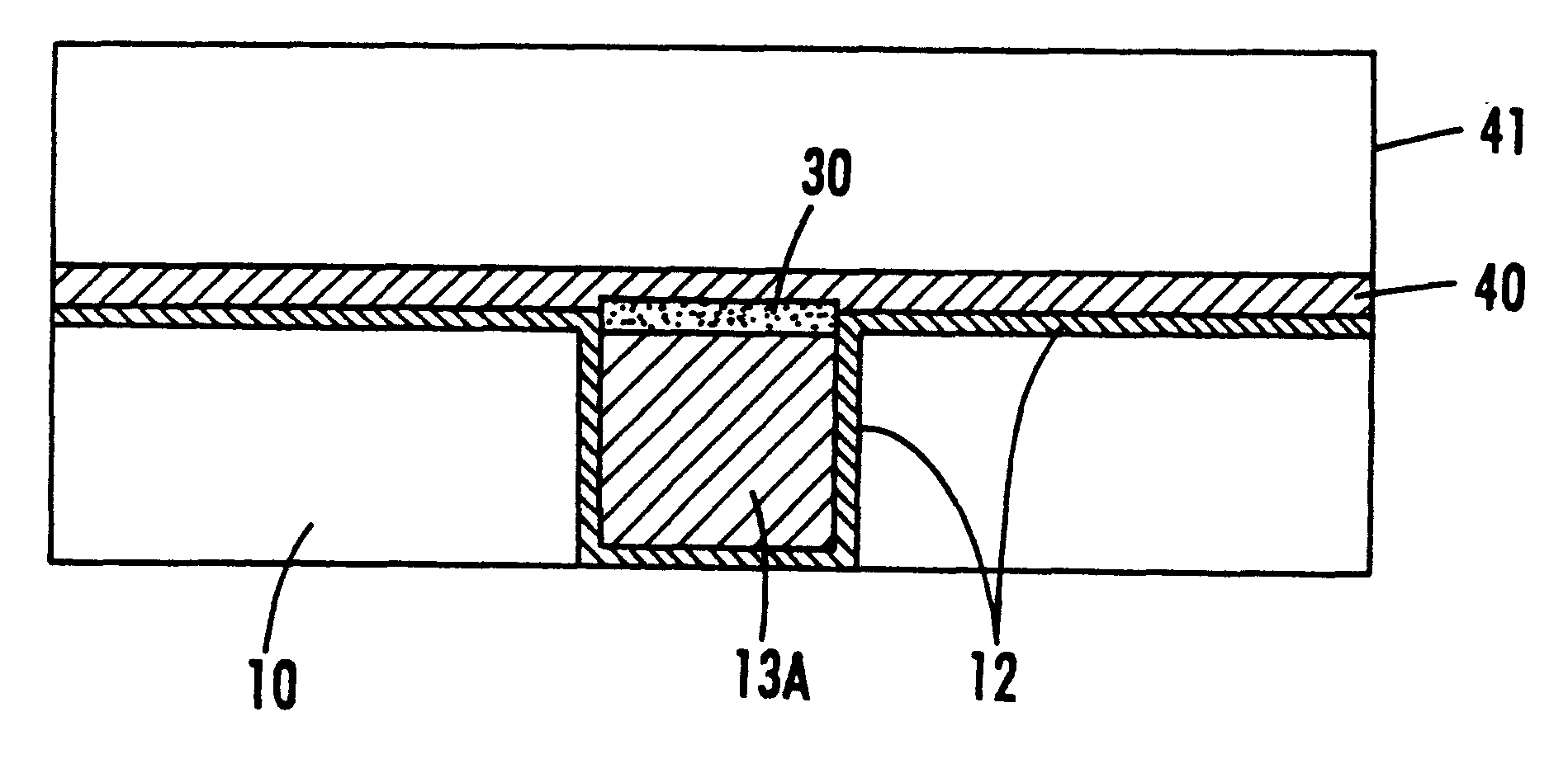
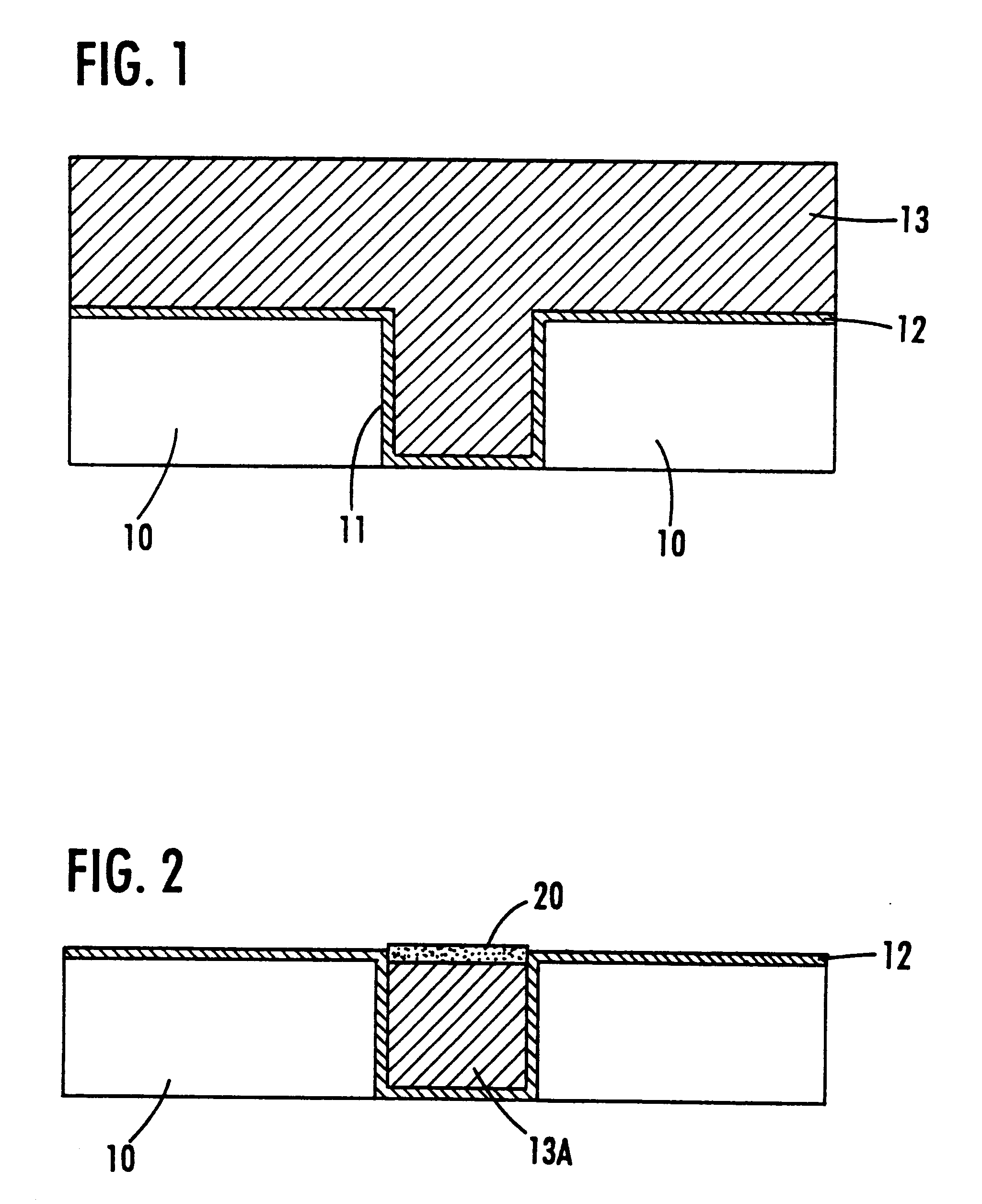
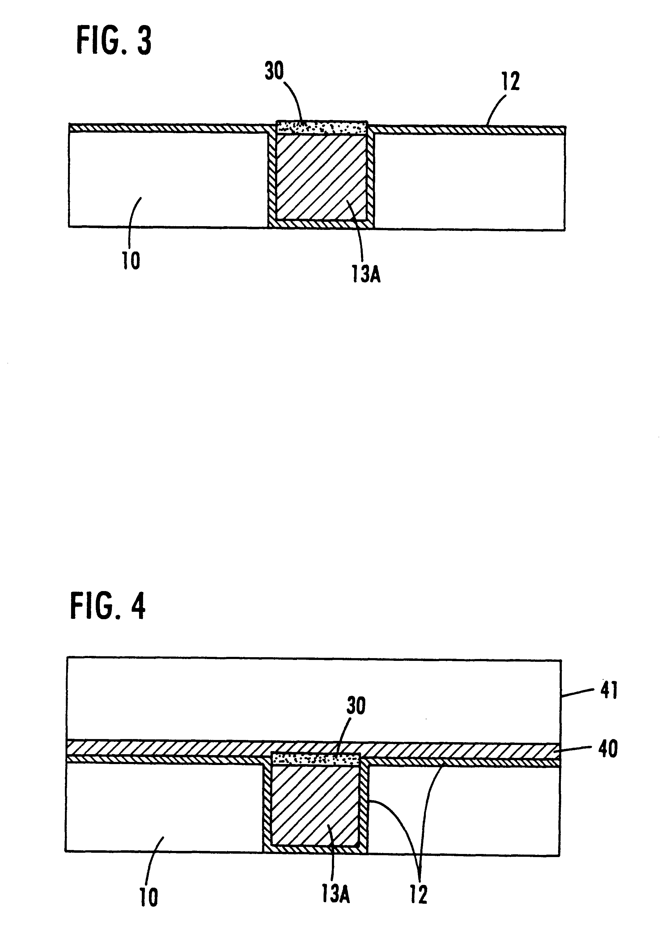
The present invention addresses and solves problems attendant upon capping Cu and / or Cu alloy interconnect members, as with a capping layer of silicon nitride. The present invention advantageously enables increased adhesion of a capping layer, such as silicon nitride, to a Cu or Cu alloy interconnect member, thereby preventing copper diffusion and enhancing electromigration resistance.

As design rules are scaled down into the deep submicron range, e.g., about 0.18 microns and under, the reliability of encapsulated Cu and / or Cu alloy interconnect members becomes increasingly significant. It was found that conventional practices in forming a Cu or Cu alloy interconnect member in a damascene opening results in the formation of a thin copper oxide surface film, believed to comprise a mixture of CuO and Cu.sub.2 O. It is believed that such a thin copper oxide surface film forms during CMP. The thin copper oxide surface film is porous and brittle in nature. The presence of such a thin copp...


PUM


Abstract

The adhesion of a diffusion barrier or capping layer to Cu and/or Cu alloy interconnect members is significantly enhanced by treating the exposed surface of the Cu and/or Cu alloy interconnect members with a silane or dichlorosilane plasma to form a layer of copper silicide thereon prior to depositing the capping layer. Embodiments include electroplating or electroless plating Cu or a Cu alloy to fill a damascene opening in a dielectric interlayer, chemical mechanical polishing, treating the exposed surface of the Cu or Cu alloy interconnect member in a silane or dichlorosilane plasma to form the copper silicide layer and depositing a capping layer of silicon nitride thereon.

Description

TECHNICAL BACKGROUNDThe present invention relates to copper (Cu) and / or Cu alloy metallization in semiconductor devices. The present invention is applicable to manufacturing high speed integrated circuits having submicron design features and high conductivity interconnect structures.The escalating requirements for high density and performance associated with ultra large scale integration semiconductor wiring require responsive changes in interconnection technology, which is considered one of the most demanding aspects of ultra large scale integration technology. Such escalating requirements have been found difficult to satisfy in terms of providing a low RC (resistance capacitance) interconnect pattern, particularly wherein submicron vias, contacts and trenches have high aspect ratios imposed by miniaturization.Conventional semiconductor devices comprise a semiconductor substrate, typically doped monocrystalline silicon, and a plurality of sequentially formed dielectric interlayers ...

Claims


Application Information

Patent Timeline
IPC IPC(8): H01L21/768H01L21/70H01L23/532H01L23/52
CPCH01L21/76834H01L21/76849H01L23/53233H01L23/53238H01L2924/0002H01L2924/00
Inventor NGO, MINH VANPRAMANICK, SHEKHARNOGAMI, TAKESHI
Owner GLOBALFOUNDRIES INC
Why Eureka
Try Eureka