

Method for heat treatment of SOI wafer and SOI wafer heat-treated by the method
a technology of soi wafer and heat treatment method, which is applied in the direction of basic electric elements, electrical apparatus, and semiconductor devices, can solve the problems of increasing production costs, adversely affecting the active layer in the vicinity, and forming pits, so as to improve device characteristics and yield, reduce the number of cops in the surface layer portion of the soi layer, and improve the yield
Inactive Publication Date: 2001-05-29
SHIN-ETSU HANDOTAI CO LTD
View PDF8 Cites 20 Cited by
- Summary
- Abstract
- Description
- Claims
- Application Information
AI Technical Summary
Benefits of technology
The present invention has been accomplished to solve the above-mentioned problems, and an object of the invention is to provide a method for heat treatment which eliminates COPs in an SOI layer in accordance with a hydrogen annealing method, while preventing etching of the SOI layer and a buried oxide layer; i.e., formation of pits.
In contrast with the conventional batch type heat treatment, the heat treatment according to the present invention utilizes a single-wafer type RTA, so that a wafer can be heat-treated within a short period of time to thereby provide a mass-producing effect. Further, since the amount of hydrogen gas to be used decreases, safety in relation to operation can be secured.
Problems solved by technology
They also found that defects such as COPs (Crystals Originated Particles) are present in the SOI layer and that when such defects extend to a substrate oxide film, there occurs a disadvantageous phenomenon such that the COPs remain uneliminated or may even expand and that the buried oxide layer is etched by hydrogen that invades into the oxide layer through defects, resulting in formation of pits and adversely affecting the active layer in the vicinity thereof.
This method has a drawback of necessity for a step of reducing the thickness of the SOI layer after heat treatment in order to obtain an SOI layer having a thickness of 0.5 .mu.m or less.
This method can reliably eliminate defects but greatly increases production costs.
Further, the above-described hydrogen annealing method is described as requiring at least one hour for high temperature heat treatment, with the result that the productivity is low.
Further, since the heat treatment is performed in a batch scheme using a vertical type furnace, a large amount of hydrogen must be caused to flow through the furnace, thereby increasing danger involved in the use of hydrogen.
Meanwhile, presence of COPs has recently been reported to be a cause of decreasing the yield of a device fabricating process.
Further, COPs are said to adversely affect a device fabrication process.
That is, if COPs are present on the surface of an SOI wafer, steps are formed during a wiring process, which causes breakage of wires, resulting in decreased yield.
Method used
View moreImage
Smart ImageViewing Examples

Examples
examples
The present invention will next be described by way of example, which should not be construed as limiting the invention.
Login to View More PUM
| Property | Measurement | Unit |
|---|---|---|
| temperature | aaaaa | aaaaa |
| surface roughness | aaaaa | aaaaa |
| thickness | aaaaa | aaaaa |
Abstract
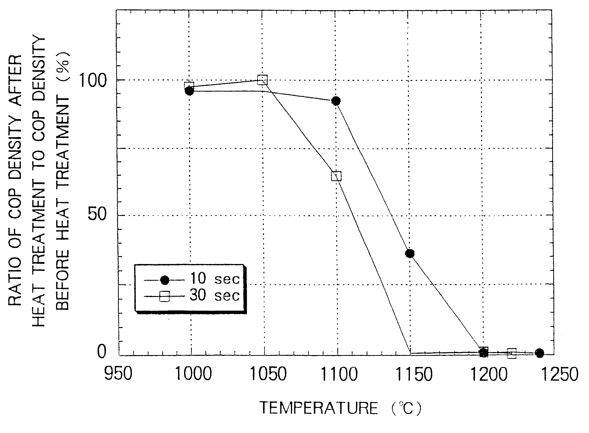
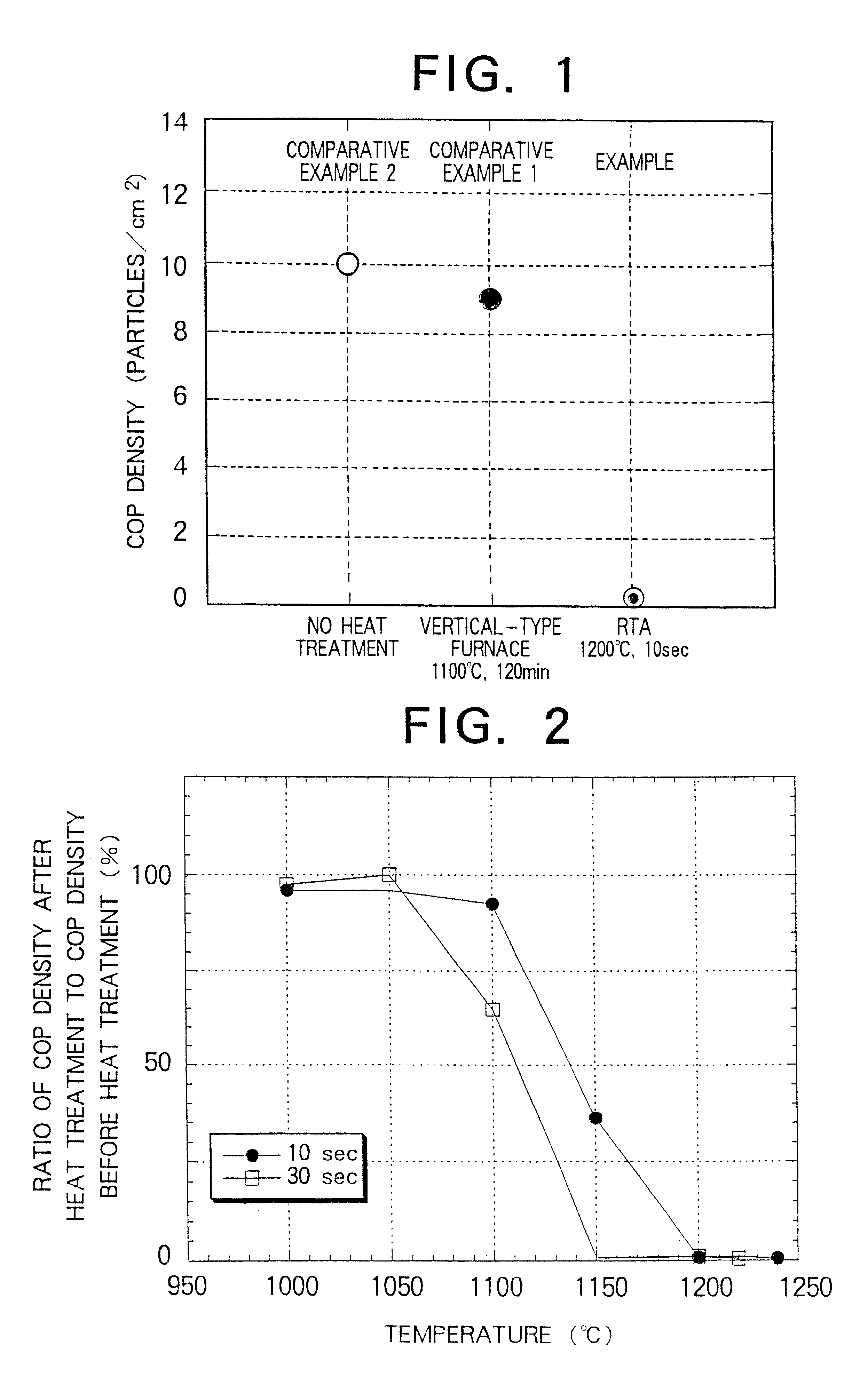
A method for heat-treating an SOI wafer in a reducing atmosphere, wherein the SOI wafer is heat-treated through use of a rapid thermal annealer at a temperature within the range of 1100.degree. C. to 1300.degree. C. for 1 sec to 60 sec. The reducing atmosphere is preferably an atmosphere of 100% hydrogen or a mixed gas atmosphere containing hydrogen and argon. The heat treatment is preferably performed for 1 sec to 30 sec. The method eliminates COPs in an SOI layer of an SOI wafer in accordance with a hydrogen annealing method, while preventing etching of the SOI layer and a buried oxide layer.
Description
BACKGROUND OF THE INVENTION1. Field of the InventionThe present invention relates to a method for heat treatment of an SOI wafer, and particularly to a method for heat treatment capable of reducing crystal originated particle (hereinafter referred to as COP) density in the surface of an SOI layer while preventing etching of the SOI layer and a buried oxide layer.2. Description of the Related ArtThere has been proposed a technique such that an SOI (Silicon on Insulator) wafer is heat-treated at 500-1200.degree. C. in a reducing atmosphere of 200 Torr or less in order to improve the surface roughness of the SOI wafer (see Japanese Patent Application Laid-Open (kokai) No. 5-217821). This patent publication states that when an SOI wafer is heat-treated at 950.degree. C. in a hydrogen atmosphere of 80 Torr or less, the surface roughness of the SOI layer is improved from 20 nm to 1.5 nm.In this case, the SOI layer of the SOI wafer is formed from an epitaxial layer.Meanwhile, through perfo...
Claims
Login to View More Application Information
Patent Timeline
 Patent Type & AuthorityPatents(United States)
IPC IPC(8): H01L21/02H01L21/322H01L21/324H01L21/70H01L21/762H01L21/316H01L27/12
CPCH01L21/3226H01L21/324H01L21/76256H01L21/20
InventorAGA, HIROJIKOBAYASHI, NORIHIROMITANI, KIYOSHI
OwnerSHIN-ETSU HANDOTAI CO LTD