Environment exchange control for material on a wafer surface

a technology of environment exchange control and material, applied in the field of microelectronic fabrication, can solve the problems of reducing the moisture content below, obtaining the maximum performance of these sensitive photoresists, and sensitive to the chemical environmen

Inactive Publication Date: 2001-07-03
ASML HLDG NV
View PDF10 Cites 33 Cited by
  • Summary
  • Abstract
  • Description
  • Claims
  • Application Information

AI Technical Summary

Benefits of technology

A method or apparatus, representing an embodiment of the invention, can be cost effective and advantageous for at least the following reasons. This invention improves the lithographic performance and process control of the ACETAL-based or any environmentally sensitive DUV photoresists and improves their chances of being successfully used for smaller feature sizes. This invention provides a way to eliminate / minimize outgassing of the ACETAL-based or any environmentally sensitive photoresists during the exposure step, thereby preventing contamination of the projection optics of exposure tools. This invention improves the mechanical and physical properties of low dielectric constant liquid polymeric films. This invention helps to prevent contamination of stepper optics.All the disclosed embodiments of the invention described herein can be realized and practiced without undue experimentation. Although the best mode of carrying out the invention contemplated by the inventors is disclosed above, practice of the invention is not limited thereto. Accordingly, it will be appreciated by those skilled in the art that the invention may be practiced otherwise than as specifically described herein.For example, the individual components need not be formed in the disclosed shapes, or assembled in the disclosed configuration, but could be provided in virtually any shape, and assembled in virtually any configuration. Further, the individual components need not be fabricated from the disclosed materials, but could be fabricated from virtually any suitable materials. Further, although the enclosed thermal chamber described herein can be a physically separate module, it will be manifest that the enclosed thermal chamber may be integrated into the apparatus with which it is associated. Furthermore, all the disclosed elements and features of each disclosed embodiment can be combined with, or substituted for, the disclosed elements and features of every other disclosed embodiment except where such elements or features are mutually exclusive. It will be manifest that various additions, modifications and rearrangements of the features of the invention may be made without deviating from the spirit and scope of the underlying inventive concept. It is intended that the scope of the invention as defined by the appended claims and their equivalents cover all such additions, modifications, and rearrangements. The appended claims are not to be interpreted as including means-plus-function limitations, unless such a limitation is explicitly recited in a given claim using the phrase "means-for." Expedient embodiments of the invention are differentiated by the appended subclaims.

Problems solved by technology

The problems encountered in obtaining the maximum performance out of these sensitive photoresists is known to those skilled in the art of photolithography.
One problem with ACETAL-based photoresists is that they are very sensitive to the chemical environment throughout the lithography process sequence.
If the previous post application bake (PAB) process conditions and the stepper environment are not carefully optimized, and film moisture content decreases below a certain value, the ultimate lithographic performance of these photoresists will deteriorate significantly.
The second problem with the ACETAL-based chemistries is that deblocking reaction rate of an ACETAL-based resist is much faster than the less sensitive DUV chemistries such as T--BOC resists due to a weak H--O physical bond.
This is why the deblocking reaction starts at room temperature, thus causing contamination of the projection optics of the exposure tools (step and scanner) during the exposure step.
Heretofore, the requirements of obviating moisture and temperature sensitivity referred to above have not been fully met.

Method used


Image

  • Environment exchange control for material on a wafer surface
  • Environment exchange control for material on a wafer surface
  • Environment exchange control for material on a wafer surface

Examples


first embodiment

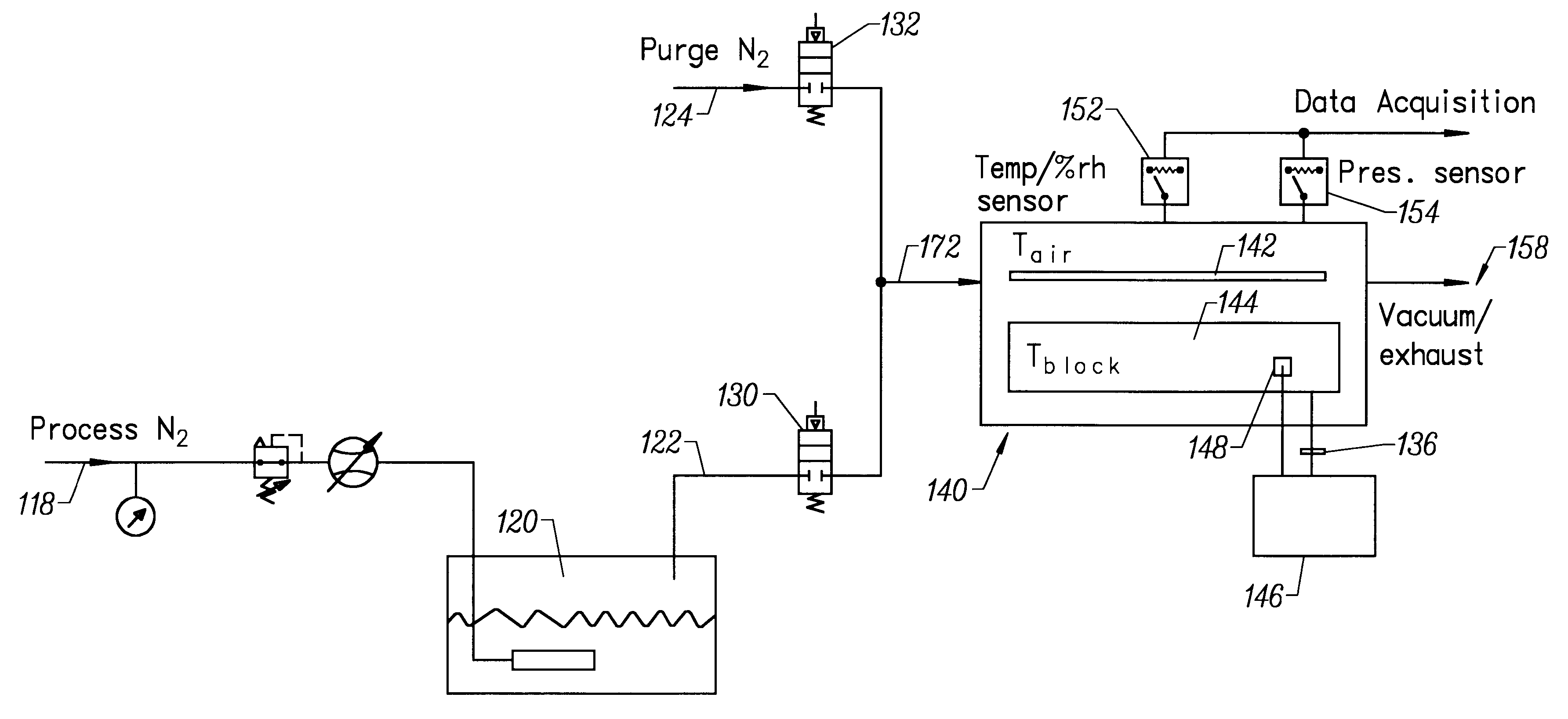
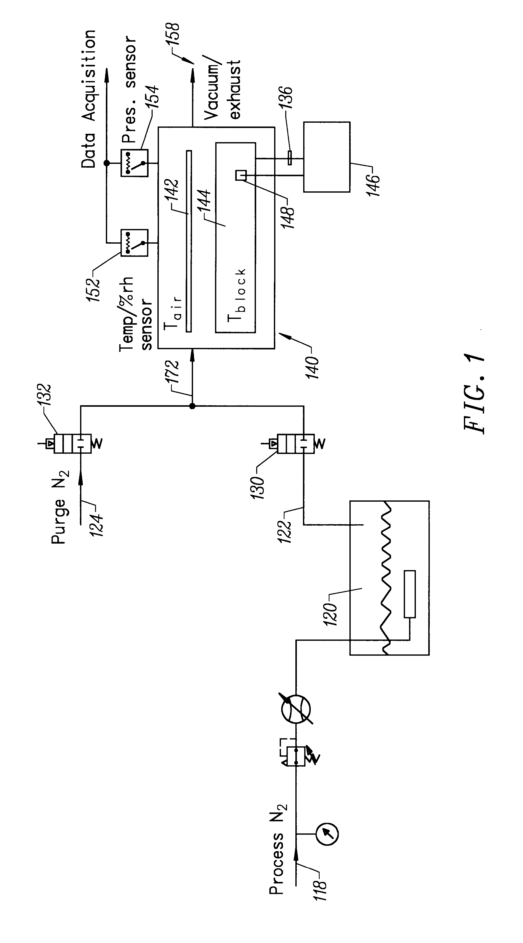
After forming a DUV resist coat on a wafer, the wafer and the coating may be dehydrated within a wafer processing chamber that is being utilized as a post application bake (PAB)module. This involves controlling an exchange between the polymer coating and a surrounding environment defined by the wafer-processing chamber. Specifically, drawing moisture out of the environment will cause the amount of available water on the surface of the polymer to be reduced as this water exchanges to the environment in an attempt to achieve equilibrium. A gaseous mixture such as N.sub.2 may be introduced into the wafer processing chamber so that the wafer processing chamber dehydrates the DUV resist coat. The wafer may then be exposed in a normal manner by a stepper and / or scanner tool. Since the resist coat material has been dehydrated before entering the exposure part of the process, only a minute amount of deprotection will take place, during the exposure. As such, the outgas during exposure is mi...

second embodiment

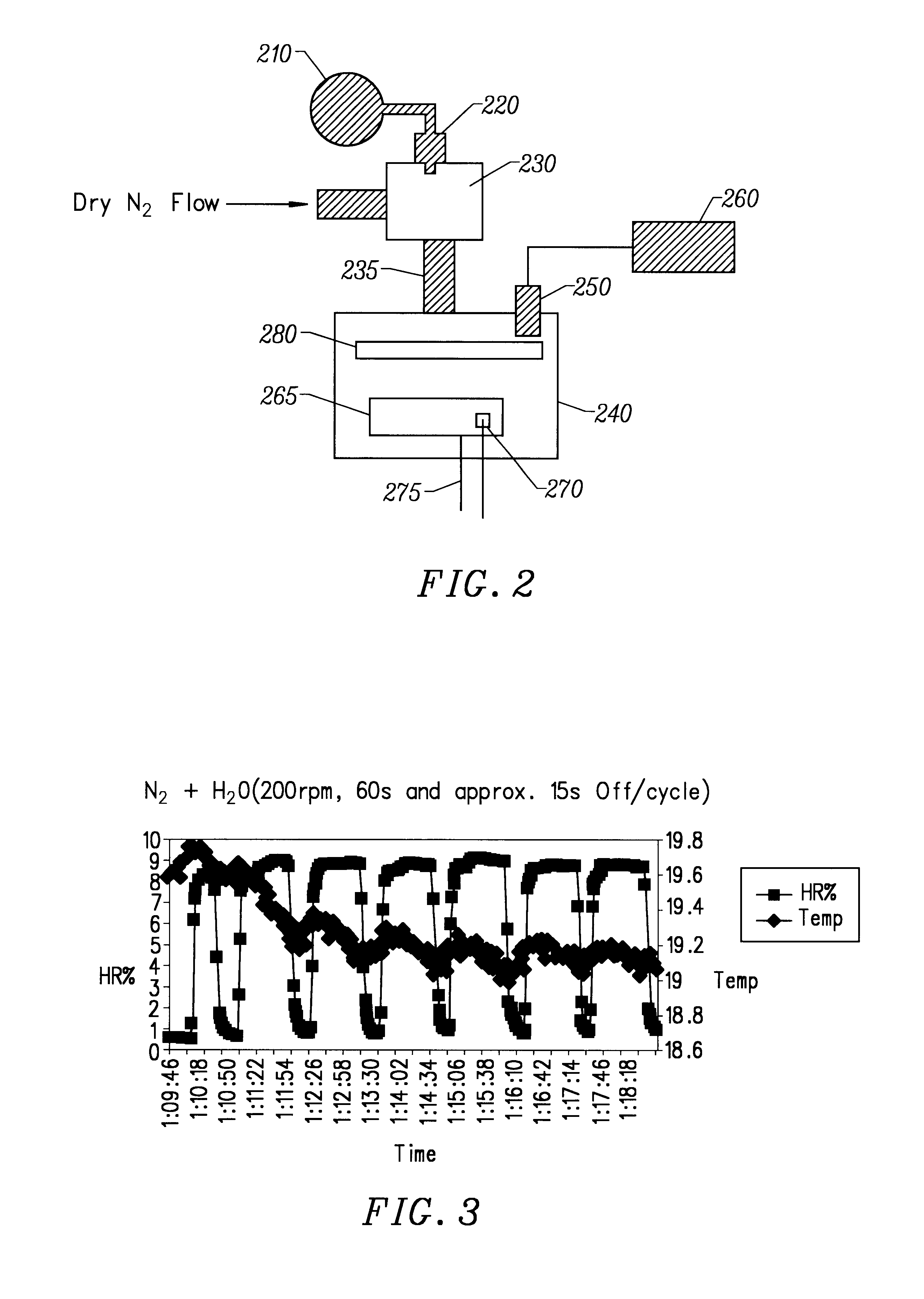
In second embodiment, an ACETAL DUV coated wafer is treated in an environmentally controlled chamber forming a bake unit during a post application sub-step. The chamber regulates a known amount of solvent, moisture or chemical(s) for the purpose of treating the wafer in a controlled fashion. In this embodiment the controlled exchange with the surface of the polymer is limited to the time during which the wafer is located in the environment defined by the PAB unit. Under these conditions, the final performance of the ACETAL resist may be enhanced. In comparison with the prior without any change of resist chemistry or exposure tool.

third embodiment

In a third embodiment the wafer is treated once after the wafer is exposed. More specifically, after the DUV coated wafer is photolithographically exposed in the stepper, the wafer is transferred to an environmentally controlled chamber forming a PEB unit. In the chamber, a known amount of solvent, moisture or chemical is regulated to treat the wafer in a controlled fashion. In this embodiment, the controlled exchange between the environment and the polymer is limited to the time in which the wafer is located in the PEB unit. Under these conditions, the final performance of the ACETAL resist may be enhanced in comparison to the prior art without any change of resist chemistry or exposure tool.


PUM

PropertyMeasurementUnit
dielectric constantaaaaaaaaaa

Abstract

Systems and methods are described for environmental exchange control for a polymer on a wafer surface. An apparatus for controlling an exchange between an environment and a polymer on a surface of a wafer located in the environment includes: a chamber adapted to hold the wafer, define the environment, and maintain the polymer in an adjacent relationship with the environment; and a heater coupled to the chamber. A method for improving performance of a spin-on material includes: forming the spin-on material on a surface of a wafer; then locating the spin-on material in an environment so that said environment is adjacent said spin-on material; and then controlling an exchange between the spin-on material and said environment. The systems and methods provide advantages because inappropriate deprotection is mitigated by careful control of the environmental temperature and environmental species partial pressures (e.g. relative humidity).

Description

1. Field of the InventionThe invention relates generally to the field of microelectronic fabrication. More particularly, the invention relates to the fabrication of polymeric microelectronic structures, such as photoresist masks and low dielectric constant materials.2. Discussion of the Related ArtThe manufacturing of advanced semiconductors requires the production of circuit features at the sub micron level. A very sensitive photoresist is needed to define these features. The problems encountered in obtaining the maximum performance out of these sensitive photoresists is known to those skilled in the art of photolithography.A class of new generation deep ultra-violet (DUV) chemically amplified photoresists based on "ACETAL" chemistry is required to produce features between 0.10-0.25 um using an exposure wavelength of 248 nm. One problem with ACETAL-based photoresists is that they are very sensitive to the chemical environment throughout the lithography process sequence. This is due...

Claims


Application Information

Patent Timeline
Patent Type & Authority Patents(United States)
IPC IPC(8): G03F7/38G03F7/26G03F7/20G03F7/16G03F7/039H01L21/027
CPCG03F7/168G03F7/70866G03F7/38G03F7/26G03F7/16G03F7/004G03F7/162H01L21/0273
Inventor GURER, EMIRLEE, ED C.ZHONG, TOMGOLDEN, KEVINLEWELLEN, JOHN W.REYNOLDS, REESEWACKERMAN, SCOTT C.
Owner ASML HLDG NV
Why Eureka
Try Eureka