
Silicon nitride barrier for capacitance maximization of tantalum oxide capacitor

Inactive Publication Date: 2001-07-10
NOVELLUS SYSTEMS
View PDF3 Cites 23 Cited by
  • Summary
  • Abstract
  • Description
  • Claims
  • Application Information

AI Technical Summary

Benefits of technology

The present invention uses a high density plasma (HDP) nitridation method to produce a high quality silicon nitride layer for separating a tantalum oxide layer in a capacitor from the conductive surfaces on either side of the tantalum oxide. A particular benefit of using the HDP process is the elimination of the more costly RTN process and the improved wafer throughput.
In the most highly preferred implementation of the method, the steps of contamination cleaning and growing a first silicon nitride layer are both completed in the same chamber without removing the conductive surface from the chamber. This speeds processing as compared to RTN processing.

Problems solved by technology

Such stack dielectrics are beginning to reach the practical limit of how thin they may be deposited.
A problem with the use of tantalum oxide, however, is that the tantalum oxide deposition process results in the formation of a thin silicon oxide interface when the tantalum oxide is deposited directly on a polysilicon bottom electrode.
This silicon oxide interface reduces the overall capacitance and degrades device functionality.
The RTN process, however, is a relatively slow and costly process.
This results from the multiple processing steps required.
Further, the RTN process results in a nitride layer that is not uniformly thick.
This adversely affects the performance of the capacitor being constructed.

Method used


Image

  • Silicon nitride barrier for capacitance maximization of tantalum oxide capacitor
  • Silicon nitride barrier for capacitance maximization of tantalum oxide capacitor

Examples


Embodiment Construction

)

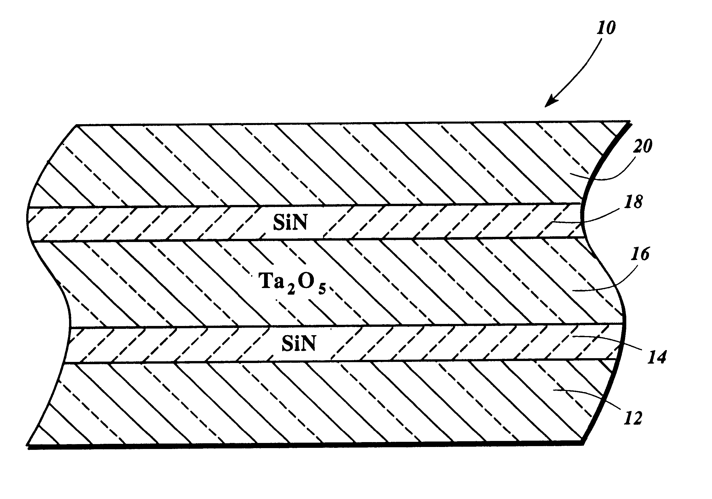
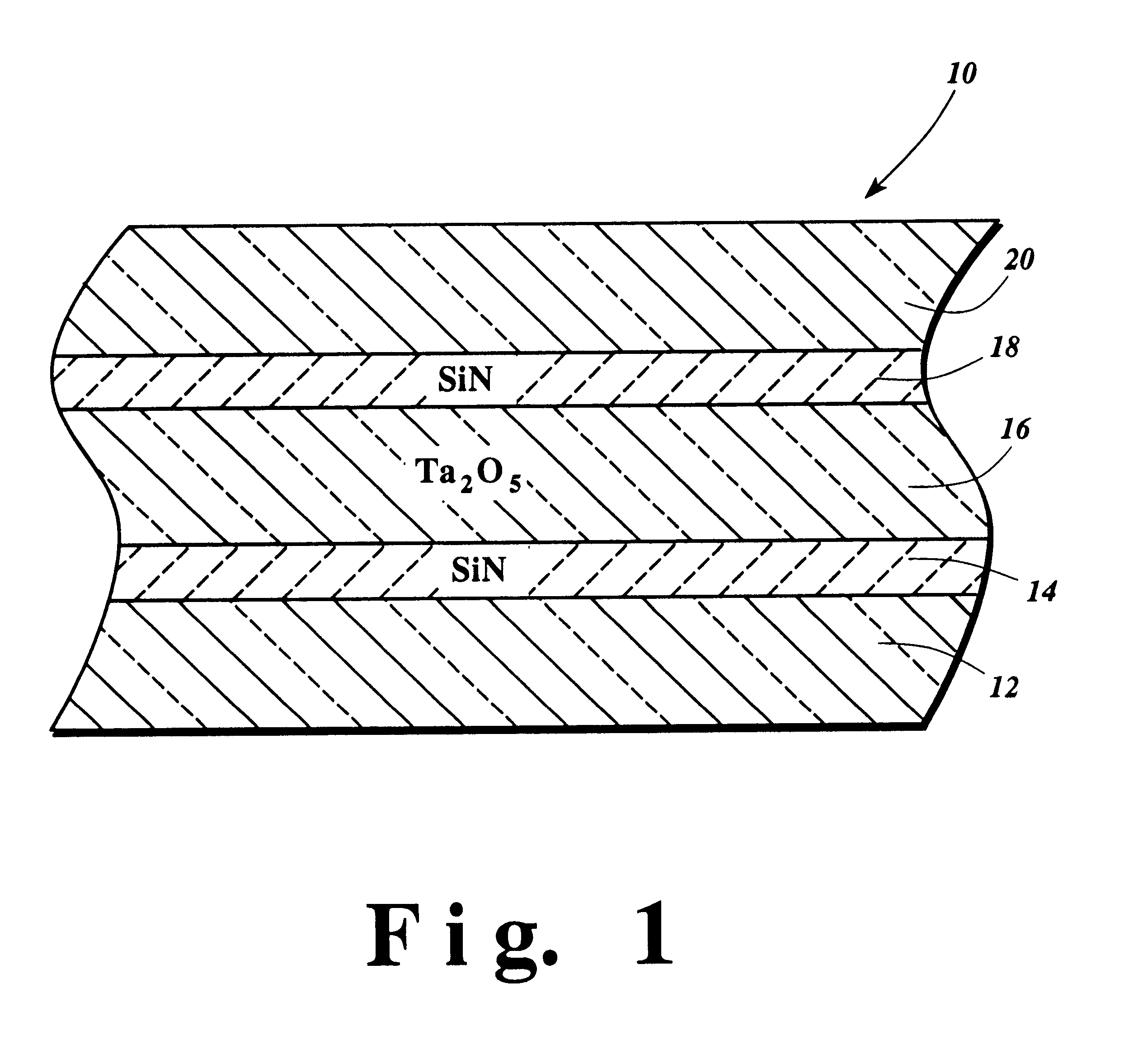
In describing the preferred embodiment of the present invention, reference will be made herein to FIG. 1. Features of the invention are not necessarily shown to scale in this drawing.

FIG. 1 shows a cross-section through a capacitor 10 constructed on a conductive surface 12 according to the method of this invention. The surface 12 acts as a lower capacitor plate. The capacitor 10 includes a first silicon nitride layer 14 separating the conductive surface 12 from the capacitor dielectric layer 16. The capacitor dielectric layer 16 is formed of tantalum oxide (Ta.sub.2 O.sub.5). A second silicon nitride layer 18 separates the capacitor dielectric layer 16 from an overlying conductive layer 20 which forms the upper capacitor plate.

The method of this invention produces a capacitor having a very thin and uniform dielectric composed of the two silicon nitride layers 14, 16, and the tantalum oxide layer 16. The method begins by contamination cleaning the exposed conductive surface 12 in a ...


PUM


Abstract

A method of making a capacitor on a conductive surface, preferably on a polysilicon surface includes contamination cleaning the surface with a high density plasma (HDP) of a first gaseous agent, such as hydrogen, then growing a silicon nitride barrier layer on the surface using a high density plasma (HDP) of nitrogen. A layer of tantalum oxide is then deposited on the silicon nitride layer to form a capacitor dielectric layer. A second silicon nitride layer is then grown on the capacitor dielectric layer, also using an HDP nitrogen plasma with the addition of a silicon containing gas, such as silane. Finally, a conductive layer is deposited on the second silicon nitride layer to form the capacitor. The HDP plasma is heated using an inductively coupled radio frequency generator. The invention also includes a capacitor constructed on a conductive surface by the method of the invention.

Description

1. Field of the InventionThe present invention relates to capacitors formed on conductive surfaces, preferably silicon surfaces, during the construction of integrated circuits. More specifically, the present invention relates to a method of making a capacitor in which silicon nitride barriers are formed between conductive surfaces forming the plates of a capacitor and a capacitor dielectric layer of tantalum oxide located between the conductive surfaces.2. Description of Related ArtAs the memory size of dynamic random access memory (DRAM) devices increases into the gigabit range, the dimensions of all memory structures and the space allotted on the semiconductor substrate for those structures have decreased. To produce capacitors of the necessary value within the limited space available, conventional oxide / nitride / oxide stack dielectrics have had to be constructed ever thinner and thinner. Such stack dielectrics are beginning to reach the practical limit of how thin they may be depo...

Claims


Application Information

Patent Timeline
IPC IPC(8): H01L21/02H01L21/70H01L21/314H01L21/316H01L21/8242
CPCH01L28/40H01L21/3143H01L21/31604H01L28/56H01L27/1085H01L21/02211H01L21/02301H01L21/02252H01L21/02183H01L21/0217H01L21/02247H01L21/02274H01L21/02315H01L21/022H10B12/03
Inventor CHEW, KOK HENGVAN CLEEMPUT, PATRICKKONJUH, KATHYRAVI, TIRUNELVELI SUBRAMANIAM
Owner NOVELLUS SYSTEMS
Learn More