Cold cathode field emission device and cold cathode field emission display

a cold cathode field and emission display technology, applied in the direction of screens, discharge tube main electrodes, tubes with electrostatic controls, etc., can solve the problems of in-plane deviation and deviation among lots, difficulty in formation, and variation of electron emission characteristics of electron emission portions, so as to prevent electron colliding, increase the electric field intensity, and improve the brightness

Inactive Publication Date: 2001-08-21
SONY CORP
View PDF6 Cites 16 Cited by
  • Summary
  • Abstract
  • Description
  • Claims
  • Application Information

AI Technical Summary

Benefits of technology

The field emission device according to the first aspect of the present invention preferably has a configuration in which the gate electrode comprises a first gate electrode and a second gate electrode, and the electron emission layer is formed so as to be sandwiched between the first gate electrode and the second gate electrode through a first insulating layer and a second insulating layer. In this configuration, since the electric field intensity can be increased with the first gate electrode, the second gate electrode and the electron emission layer, the field emission device can accomplish a high electron emission efficiency. The field emission device according to the first aspect of the present invention preferably has a configuration in which the resistance layer is formed in a region other than an overlapping region where the gate electrode and the electron emission layer overlap each other. In this configuration, no resistance layer having a high dielectric constant is arranged in a region where an electric field is generated, and a capacitance between wirings (i.e., stray capacitance) can be decreased.
As described above, the resistance layer works to decrease the variation or deviation of the electron emission characteristics among the field emission devices. Further, even when a constant voltage is applied to the electron emission layer of the field emission device, the current flowing in the electron emission layer sometimes fluctuates. The resistance layer can suppress the fluctuation of the current flowing in the electron emission layer in the above case as well.

Problems solved by technology

Actually, however, it is difficult to form the electron emission portions having a uniform form and uniform dimensions in the entirety of the supporting substrate having a large area, and some in-plane deviation and a deviation among lots are inevitable.
The problem with the field emission device is that the electron emission characteristics of the electron emission portions vary.
However, field emission devices having characteristics D.sub.5 and D.sub.6 do not begin to emit electrons from edges of the electron emission layer since the potential difference is lower than the threshold voltage.
There is also another problem that the electron emission characteristic of the electron emission portion comes to be non-uniform with the elapse of time.
As a result, there is caused a problem that it is difficult to display clear images with a conventional field emission device or that images cannot be stably displayed.

Method used


Image

  • Cold cathode field emission device and cold cathode field emission display
  • Cold cathode field emission device and cold cathode field emission display
  • Cold cathode field emission device and cold cathode field emission display

Examples


example 1

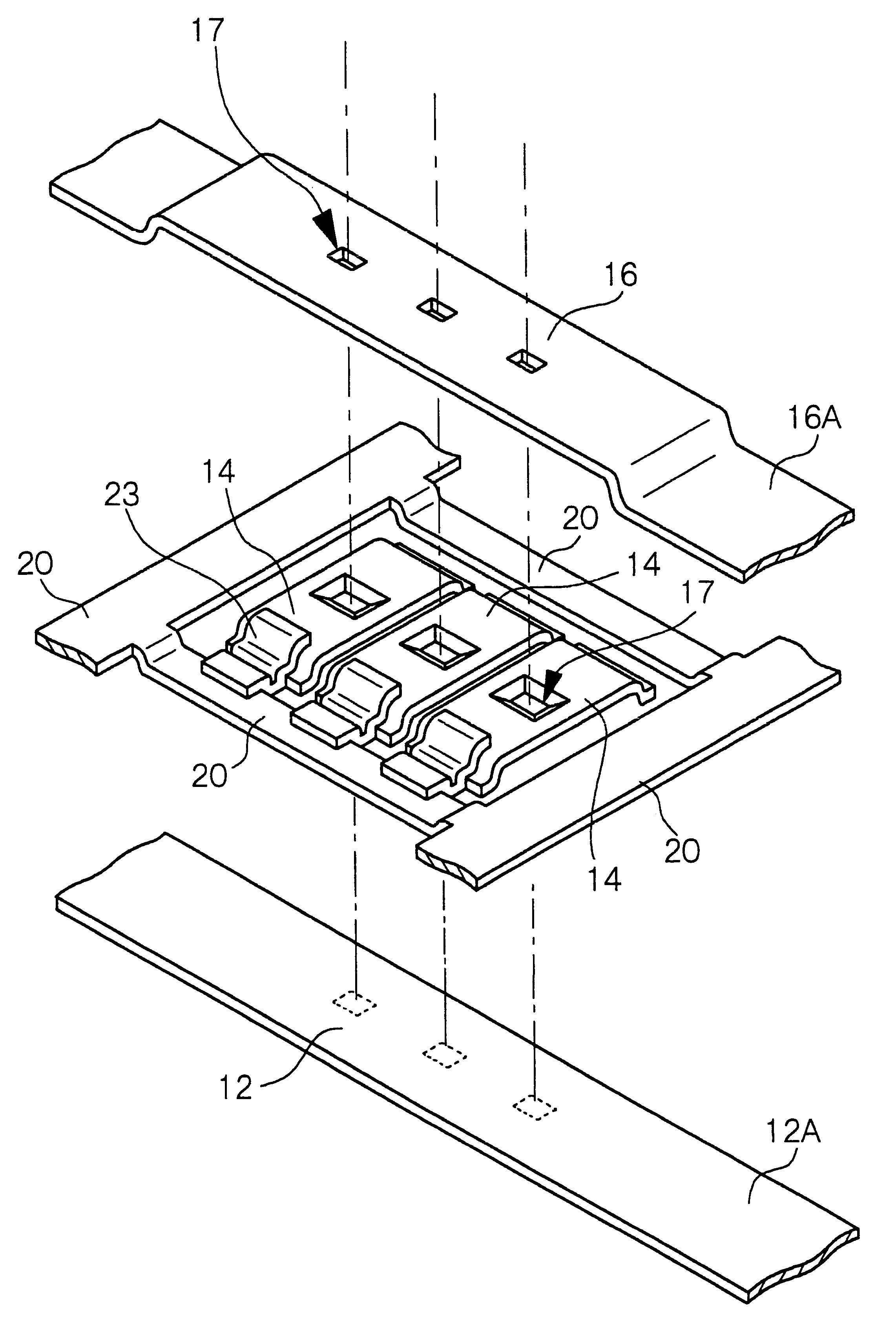
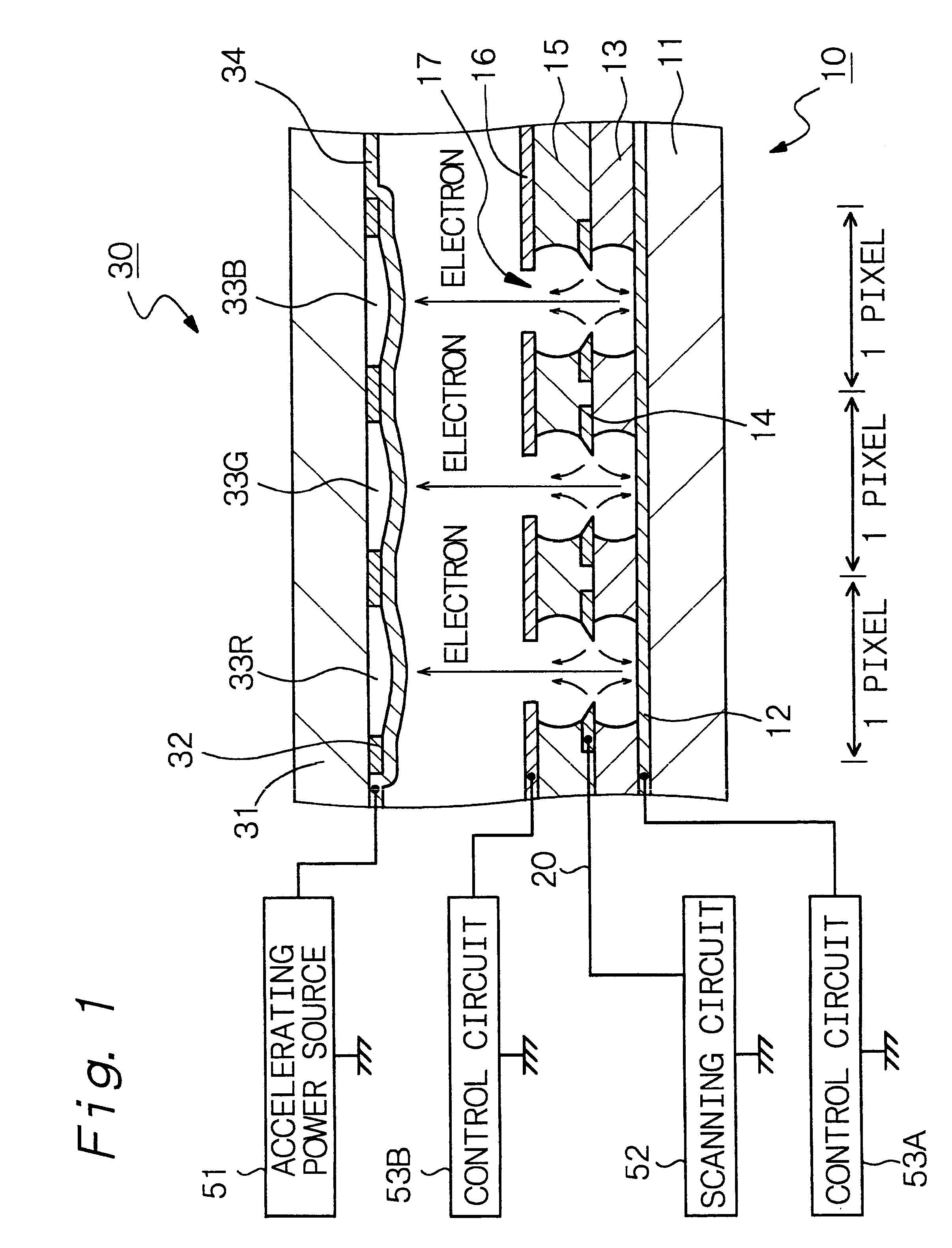
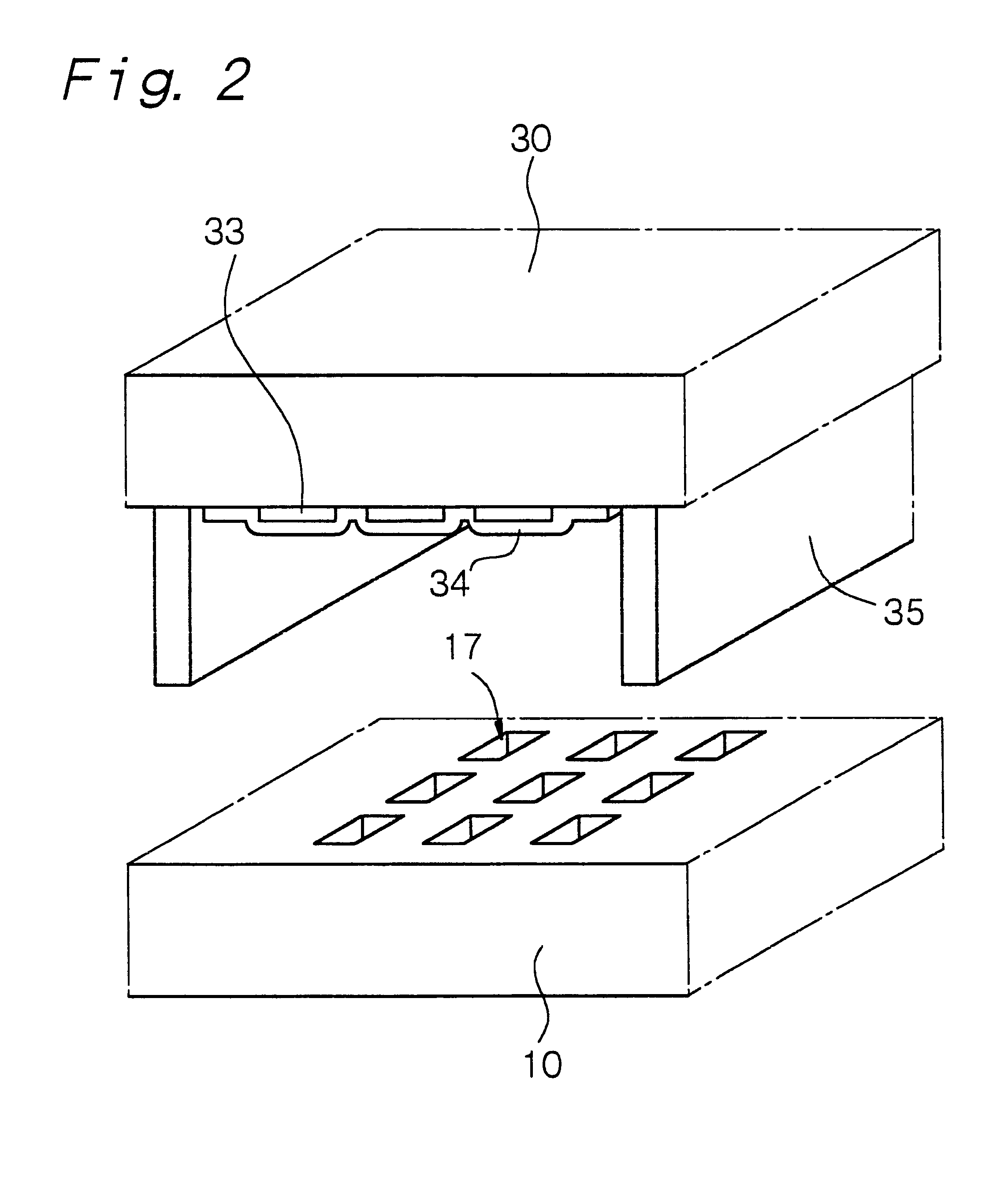
is concerned with the field emission device according to the first and second aspects of the present invention, and the display of the present invention. FIG. 1 shows a schematic partial end view of the display in Example 1, and FIG. 2 shows a conceptual view thereof. FIG. 3 shows an exploded perspective view of the field emission devices in the vicinity of the opening portions, and FIG. 4 schematically shows a configuration of elements of the field emission devices in the vicinity of the opening portions, and FIGS. 5A and 5B show schematic partial end views of the field emission devices taken along lines A--A and B--B in FIG. 4. In FIGS. 3 and 4, a supporting substrate and all of insulating layers are omitted for the convenience of showing.

The field emission device in Example 1 has a supporting substrate 11 made of, for example, a glass substrate, a first gate electrode 12, a first insulating layer 13, an electron emission layer 14, a wiring 20, a second insulating layer 15, a seco...

example 2

Example 2 is a variant of Example 1. The field emission device and the display of Example 2 differ from the counterparts of Example 1 in that the insulating interlayer 21 is omitted and that the resistance layer 23 is not formed on the insulating interlayer 21 but is formed on the electron emission layer 14, the wiring 20 and the first insulating layer 13. FIGS. 6A and 6B show schematic partial end views of the field emission device taken along lines similar to lines A--A and B--B in FIG. 4.

As shown in FIGS. 6A and 6B as well, the resistance layer 23 is directly patterned on the electron emission layer 14 and the wiring 20. The first insulating layer 13 is exposed between the electron emission layer 14 and the wiring 20 (see FIG. 6A), and the resistance layer 23 is formed on the surfaces of the first insulating layer 13, the electron emission layer 14 and the wiring 20. The connection in the above configuration can be accomplished in fewer steps than the connection through the conta...

example 3

Example 3 is a variant of Example 1 or Example 2. In Example 3, the resistance layer 23 is composed of tantalum nitride (TaN) in place of the amorphous silicon. When a film of tantalum nitride is formed by a sputtering method, tantalum nitride can be controlled to have a desired electric resistance value (for example, 6 M.OMEGA.) depending upon a sputtering apparatus and a sputtering condition. Further, tantalum nitride has a temperature coefficient of the electric resistance value .alpha. of approximately -60 ppm / .degree. C. Therefore, even at a maximum temperature (for example, 550.degree. C., a temperature at which the frit glass is sintered for bonding the cathode panel 10, the anode panel 30 and the frame with the frit glass) to which the resistance layer is exposed when the field emission devices are produced, the electric resistance value of the resistance layer is not much affected by a thermal change, and the change of the electric resistance value by temperatures is small,...


PUM


Abstract

A cold cathode field emission device having an electron emission layer (14), an insulating layer and a gate electrode (12) which are laminated one on another with the insulating layer positioned between the gate electrode, and the electron emission layer (14), and further having an opening portion which penetrates through at least the insulating layer and the electron emission layer, the electron emission layer having an edge portion for emitting electrons, the edge portion being projected on a wall surface of the opening portion, and the electron emission layer being connected to a power source through a resistance layer (23).

Description

BACKGROUND OF THE INVENTION AND RELATED ART STATEMENTThe present invention relates to a cold cathode field emission device and a cold cathode field emission display into which the cold cathode field emission device is incorporated.Various flat type, or flat panel type displays are being studied as an image display which is to replace currently main-stream cathode ray tubes (CRT). The flat type displays include a liquid crystal display (LCD), an electroluminescence display (ELD) and a plasma display panel (PDP). Further, there is also proposed a cold cathode field emission display capable of emitting electrons into a vacuum from a solid without relying on thermal excitation, and it attracts attention from the viewpoint of a brightness on a screen and a low power consumption.The cold cathode field emission display (to be sometimes simply referred to as "display" hereinafter) generally has a configuration in which a cathode panel and an anode panel are arranged so as to face each other...

Claims


Application Information

Patent Timeline
Patent Type & Authority Patents(United States)
IPC IPC(8): H01J3/02H01J29/46H01J3/00H01J29/04H01J1/304H01J31/12
CPCH01J3/022H01J29/467H01J2329/00H01J2201/30423
Inventor IWASE, YUICHIOKITA, MASAMI
Owner SONY CORP
Why Eureka
Try Eureka