Semiconductor device and production method thereof

a technology of semiconductor devices and production methods, applied in the direction of transistors, chemical vapor deposition coatings, coatings, etc., can solve the problems of high leak current between the upper and lower electrodes, degradation of the dielectric strength of the dielectric film, and inability to obtain high capacitance, etc., to achieve the effect of suppressing the increase of leak curren

Inactive Publication Date: 2001-11-13
ASAHI KASEI ELECTRONICS CO LTD
View PDF17 Cites 9 Cited by
  • Summary
  • Abstract
  • Description
  • Claims
  • Application Information

AI Technical Summary

Benefits of technology

Another object of the present invention is to provide a semiconductor device having a capacitive component that can maintain the dielectric strength without increasing the thickness of the dielectric film and suppress an increase in leak current and a production method thereof.

Problems solved by technology

However, there may be a rare case that an abnormal overvoltage is momentarily applied in addition to the rated voltage, or the dielectric film is contaminated with, for example, a metal, or defects of the film occur in the production process of the dielectric film of the capacitor, resulting in degradation of the dielectric strength of the dielectric film.
Further, as a capacitor, there is a problem in that leak current is high between the upper and lower electrodes.
However, a high capacitance cannot be obtained by the method of increasing the dielectric film thickness as used in the prior art.
Therefore, in order to obtain a high capacitance, it is necessary to increase the surface area, which results in an increased size of the semiconductor device.
Further, with increasing down-sizing requirements for semiconductor devices, if a thin film structure of the dielectric film is used to reduce the capacitor size, it is difficult to maintain the dielectric strength and suppress an increase in leak current.

Method used


Image

  • Semiconductor device and production method thereof
  • Semiconductor device and production method thereof
  • Semiconductor device and production method thereof

Examples


example 1

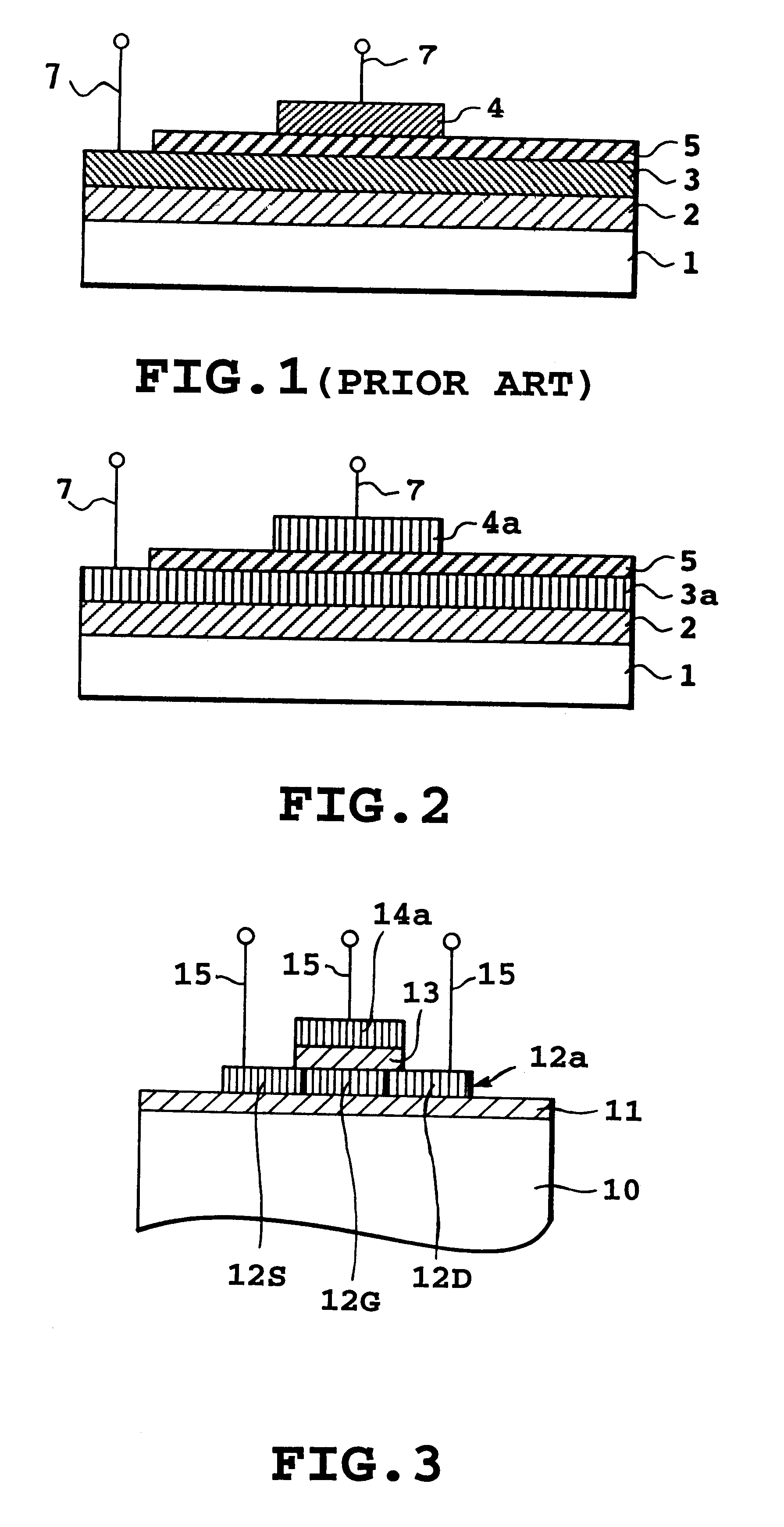
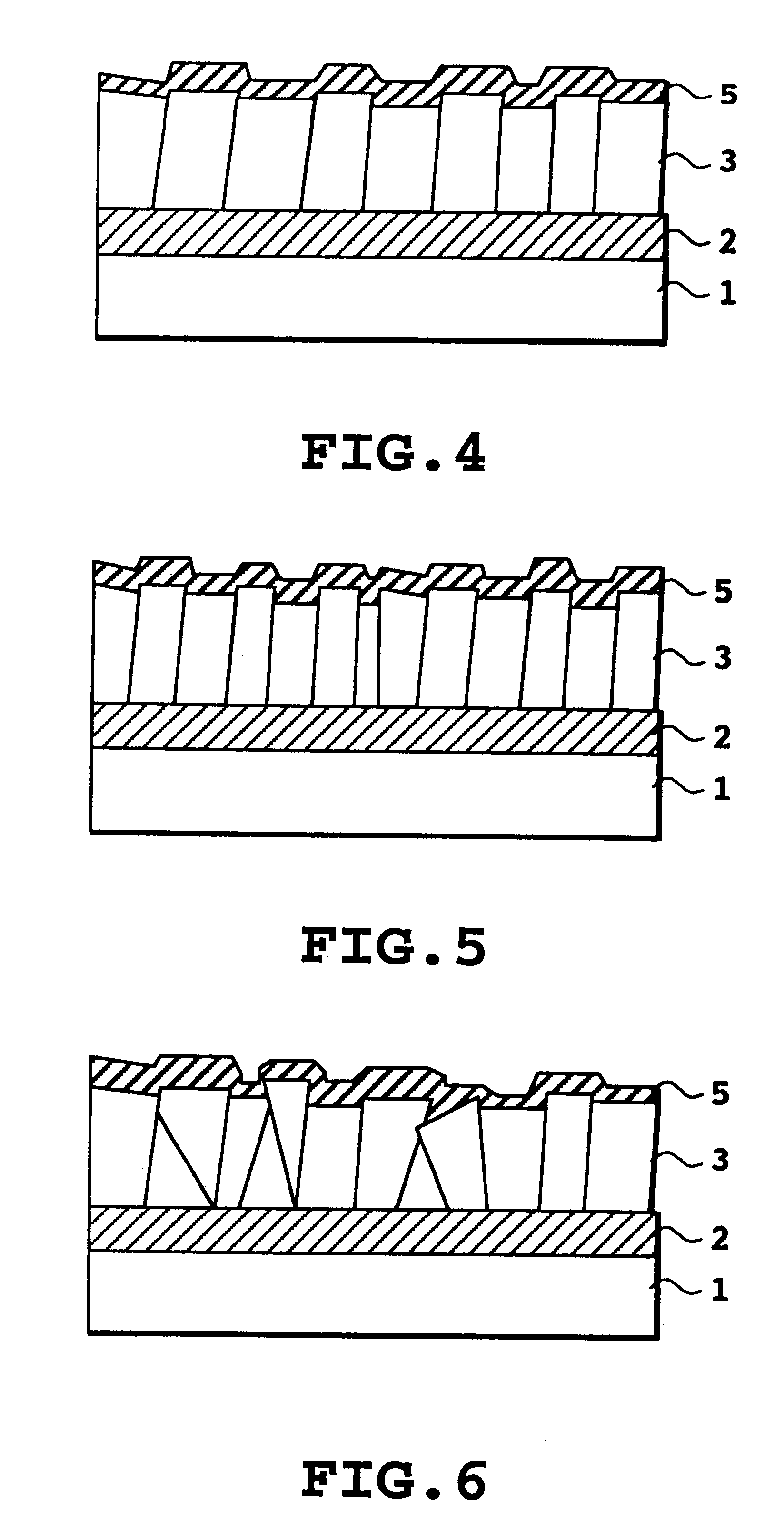
An example of the production method of the capacitor according to the present invention is illustrated in FIGS. 7A to 7E.

A silicon substrate (SiO.sub.2 / Si) formed with a silicon oxide film 2 is provided on which is formed a polycrystalline silicon film to a thickness of about 3500 .ANG. on the silicon oxide film 2 by a low pressure CVD method using a raw material gas (monosilane gas diluted with helium to 50%) under conditions of a film formation temperature of 640.degree. C., a pressure of 16 Pa (monosilane partial pressure: 8 Pa), and a film formation time of about 35 minutes (FIG. 7A).

The substrate formed with the polycrystalline silicon film 3 is heat treated while forming an oxide film in a heat treatment furnace using phosphorus oxychloride and oxygen as a source gas under conditions of 950.degree. C. for 10 minutes to form about 100 .ANG. of a phosphosilicate glass film 6 on the polycrystalline silicon film 3. The phosphorus is doped in an amount of 1.times.10.sup.20 atoms / c...

example 2

A capacitor was produced using the same procedure as in the Example 1 except that the monosilane partial pressure was set to 5 Pa.

example 3

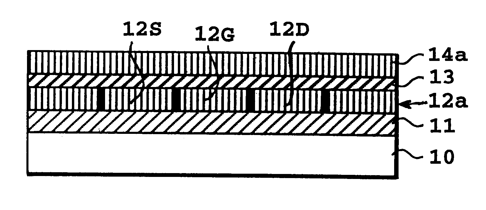
An example of the production method of the thin film transistor according to the present invention will be described with reference to FIGS. 8A to 8E.

A silicon oxide (SiO.sub.2) film 11 is formed on a silicon (Si) substrate 10, further on top of which is formed a polycrystalline silicon 12 to a thickness of about 1500 .ANG. by a low pressure CVD method using a material gas (monosilane gas diluted with helium to 50%) at a film formation temperature of 640.degree. C. and a pressure of 10 Pa (monosilane partial pressure: 5 Pa) (FIG. 8A).

The thus treated substrate is heat treated in a heat treatment furnace while forming an oxide film (phosphosilicate glass film) 16 using phosphorus oxychloride and oxygen as a source gas at a temperature of 950.degree. C. By the heat treatment, the crystal orientation of polycrystalline silicon including the gate portion (body portion) is arranged in (111) (FIG. 8B).

The phosphosilicate glass film 16 formed in step 2 is removed by etching with an HF solu...


PUM

PropertyMeasurementUnit
partial pressureaaaaaaaaaa
heightaaaaaaaaaa
temperatureaaaaaaaaaa

Abstract

On a silicon substrate 1 is provided a silicon oxide film 2, on which a polycrystalline silicon film 3 is formed by a low pressure CVD method at a monosilane partial pressure of no more than 10 Pa and a film formation temperature of no lower than 600° C. The polycrystalline silicon film is doped with an impurity such as phosphorus in a concentration of 1x10²⁰ atoms / cm3 to 1x10²¹ atoms / cm3 to form a phosphosilicate glass film 6, and after removing it, the polycrystalline silicon film is thermally oxidized in an oxidative atmosphere to form a dielectric film 5 on the surface. A polycrystalline silicon film 4 is formed on the dielectric film 5, which is treated as the oriented polycrystalline silicon film 3a to form an oriented polycrystalline silicon film 4a. The oriented polycrystalline silicon film 4a as an upper electrode and the oriented polycrystalline silicon film 3a as a lower electrode are wired to obtain a semiconductor device having a capacitor. Further, a thin film transistor of a high dielectric strength can be produced in a short time on the polycrystalline silicon which is oriented in a short time.

Description

This application is based on Patent Application No. 07-139,633 filed Jun. 6, 1995 in Japan, the content of which is incorporated fereinto by reference. In addition, this application is a continuation application of International Application No. PCT / JP96 / 01541 filed Jun. 6, 1996.The present invention relates to a semiconductor device having a dielectric film formed by thermal oxidation of polycrystalline silicon and to a production method thereof. More specifically, the present invention relates to a semiconductor device having a dielectric film formed by providing polycrystalline silicon of improved film quality, followed by thermal oxidation and to a production method thereof.DESCRIPTION OF RELATED ARTA capacitor as a component of IC and LSI is an indispensable part for IC and LSI of a specific field. In general a capacitor of IC and LSI has a structure as shown in FIG. 1 in which a dielectric film 5 is sandwiched between polycrystalline silicon films 3 and 4 on a silicon oxide fil...

Claims


Application Information

Patent Timeline
Patent Type & Authority Patents(United States)
IPC IPC(8): H01L29/02H01L29/66H01L21/02H01L21/336H01L21/28H01L29/786H01L29/04
CPCH01L21/28158H01L28/40H01L29/045H01L29/66757H01L29/78675H01L27/04
Inventor OKUSA, YOSHIHIROYAMAUCHI, TATSUYA
Owner ASAHI KASEI ELECTRONICS CO LTD
Why Eureka
Try Eureka