Light transmitting/receiving module

a light transmitting/receiving module and light transmitting technology, applied in the direction of instruments, semiconductor lasers, optical elements, etc., can solve the problems of bringing the transmission signal to the reception port as noise, the reception part has a high impedance, and the external noise of the reception por

Inactive Publication Date: 2001-11-20
SUMITOMO ELECTRIC IND LTD
View PDF3 Cites 56 Cited by
  • Summary
  • Abstract
  • Description
  • Claims
  • Application Information

AI Technical Summary

Problems solved by technology

The receiving part has a high impedance which is subject to external noise.
The reception port is subject to noise due to the weak photocurrent and the high amplification rate.
The simultaneous transmission and reception has a tendency of bringing the transmission signals to the reception port as noise.
The LD / PD (ONU) module of FIG. 4, however, is too expensive owing to many costly parts and devices.
Furthermore, there is another defect that the direction of the fiber is perpendicular to the plane of the stem (package).
This is a geometric defect which induces a difficulty for reducing the size of the module.
The PD module and the LD module are bulky and large by themselves.
The expensive metal packages for the PD, the LD, the LD driving circuit and the preamplifier raise the parts cost of the ONU module of FIG. 4.
Miniaturization of the ONU (LD / PD) module dislikes separate PD and LD which would raise the cost and the size.
Adoption of a ceramic package would lead to an expensive module despite the reduction of the number of the packages.
The large driving current required by the long-range communication induces a difficult problem of the crosstalk (or inner noise) from the LD to the PD.
Strong LD electric signals propagate in space and induce noise in the receiving part.
The receiving part of the PD and the AMP has a high input impedance and high amplification ratio which have a tendency of inviting noise.
The noise lowers the sensitivity of the receiving part.
The shorter distance between the LD and the PD / AMP brings about the more serious difficulty.
Namely, the problem of the crosstalk would become more severe, when the size of the module is reduced.
But too many and too large holes would reduce the function of shielding the receiving part from the electromagnetic noise.
But this invention does not choose the ceramic package due to the expensiveness.
If the unified module were to be stored in a ceramic package, the module would be still expensive.

Method used


Image

  • Light transmitting/receiving module
  • Light transmitting/receiving module
  • Light transmitting/receiving module

Examples


embodiment 1 (

[Embodiment 1 (Y-branch Waveguide)]

FIG. 5 to FIG. 11 demonstrate embodiment 1 having a silicon bench (platform) with a Y-branch waveguide. FIG. 5 shows a design of locations of parts on the silicon bench 42. The silicon bench 42 is prepared by making a transparent silicon dioxide (SiO.sub.2) layer upon a silicon crystal substrate by a sputtering method or an oxidization method. Doping the SiO.sub.2 layer with a dopant for raising the refractive index makes a straight waveguide 43 and a bent waveguide 44 on the Si bench 42. The adjacent parts of the waveguides form a WDM (wavelength division multiplexer: waveguide type optical coupler) 45. Aiming at the simultaneous transmission, this invention employs two different wavelengths .lambda.1 and .lambda.2. The WDM 45 has the wavelength selectivity of selecting either .lambda.1 or .lambda.2 for propagating in the waveguide 43 or 44. Metallized patterns (not shown in the figures), for example, an LD ground pattern, a PD / AMP ground pattern ...

embodiment 2 (

[Embodiment 2 (Straight Waveguide, Upward Branch, Multihole+Pillows)]

embodiment 2

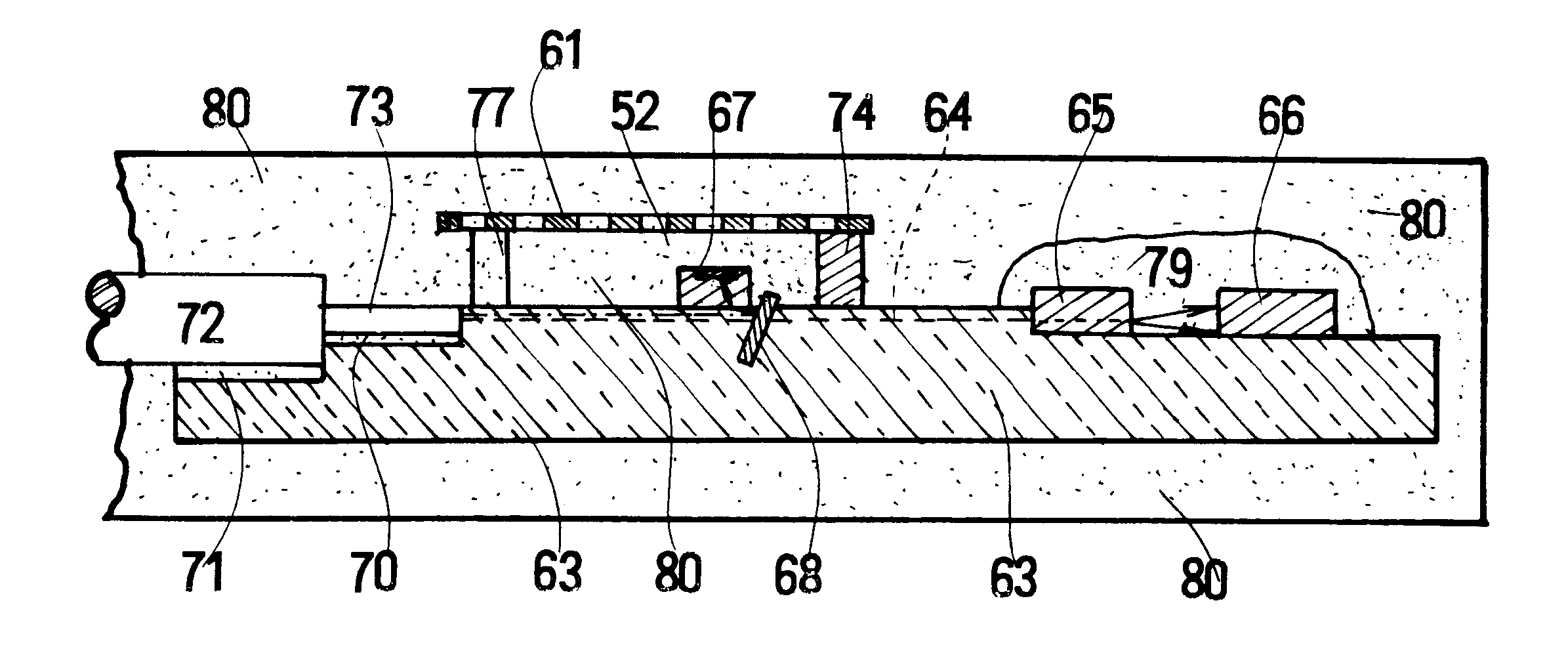
employs a straight waveguide, a WDM filter and an upward branch. FIG. 13 to FIG. 15 denote The WDM for dividing light signals into the 1.3 .mu.m and the 1.55 .mu.m is realized by a dielectric multilayer filter. FIG. 13 shows a plan view of the waveguide, devices arranged upon a silicon bench 63. The silicon bench (platform) 63 is a rectangular SiO.sub.2 (001) single crystal. The Si bench has two steps at the front part, a step at the rear part and a plateau in the middle.

The straight waveguide 64 is made in a longitudinal direction on the plateau. The device features the alignment of a PD 67 and an LD 65 along the straight waveguide 64. The LD 65 is mounted on the rear step facing directly the end of the waveguide 64. The height of the waveguide 64 coincides with the height of the emission stripe of the LD 65. A monitoring PD 66 is fixed on the rear step on an extension of the waveguide 64 for sensing the power of the LD 65. The forward-emitted light from the LD 65 propagates in th...


PUM


Abstract

Simultaneous bidirectional transmission type LD / PD module having a substrate, a signal transmitting part mounted on the substrate, a signal receiving part formed on the substrate, an end of a fiber communicating with a base station, a light waveguide coupling the fiber to the transmitting part and the receiving part, a filter separating the receiving signal light from the transmitting signal light and a resin mold package containing the substrate, the transmitting part, the receiving part, the filter and the lead frame. The receiving part is electromagnetically shielded with multihole metal members from the noise generated by the transmitting part. The resin penetrates through the holes and fully covers the receiving part.

Description

1. Field of the InventionThis invention relates to a light transmitting / receiving module, eg., to PD / LD(or LED) module having a light signal receiving part and a light signal transmitting part. This invention, in particular, proposes an improvement of an inexpensive resin-molded package for a PD / LD module for simultaneous bidirectional optical communication by light signals of different wavelengths. This invention aims at the protection of the PD port against the noise generated by the LD port in the simultaneous, bidirectional PD / LD module.2. Description of Related ArtThis application claims the priority of Japanese Patent Application No. 11-30855 (30855 / 1999) filed on Feb. 9, 1999 which is incorporated herein by reference.A prior PD / LD module has an independent laser diode (LD) module (e.g., shown in FIG. 1) and an independent photodiode (PD) module (e.g., shown in FIG. 2). The PD module is sealed in a metal package. The LD module is also sealed in another metal package. The PD mo...

Claims


Application Information

Patent Timeline
Patent Type & Authority Patents(United States)
IPC IPC(8): G02B6/42G02B6/12H01L31/0232H01S5/00H01S5/022H01S5/026H04B10/2507H04B10/40H04B10/50H04B10/524H04B10/60
CPCG02B6/4246G02B6/4277G02B2006/12164H01L2224/48091H01L2224/73265H01L2924/00014H01L2924/3011H01L2924/00H01L2924/3025
Inventor NAKANISHI, HIROMIKUHARA, YOSHIKI
Owner SUMITOMO ELECTRIC IND LTD
Why Eureka
Try Eureka