

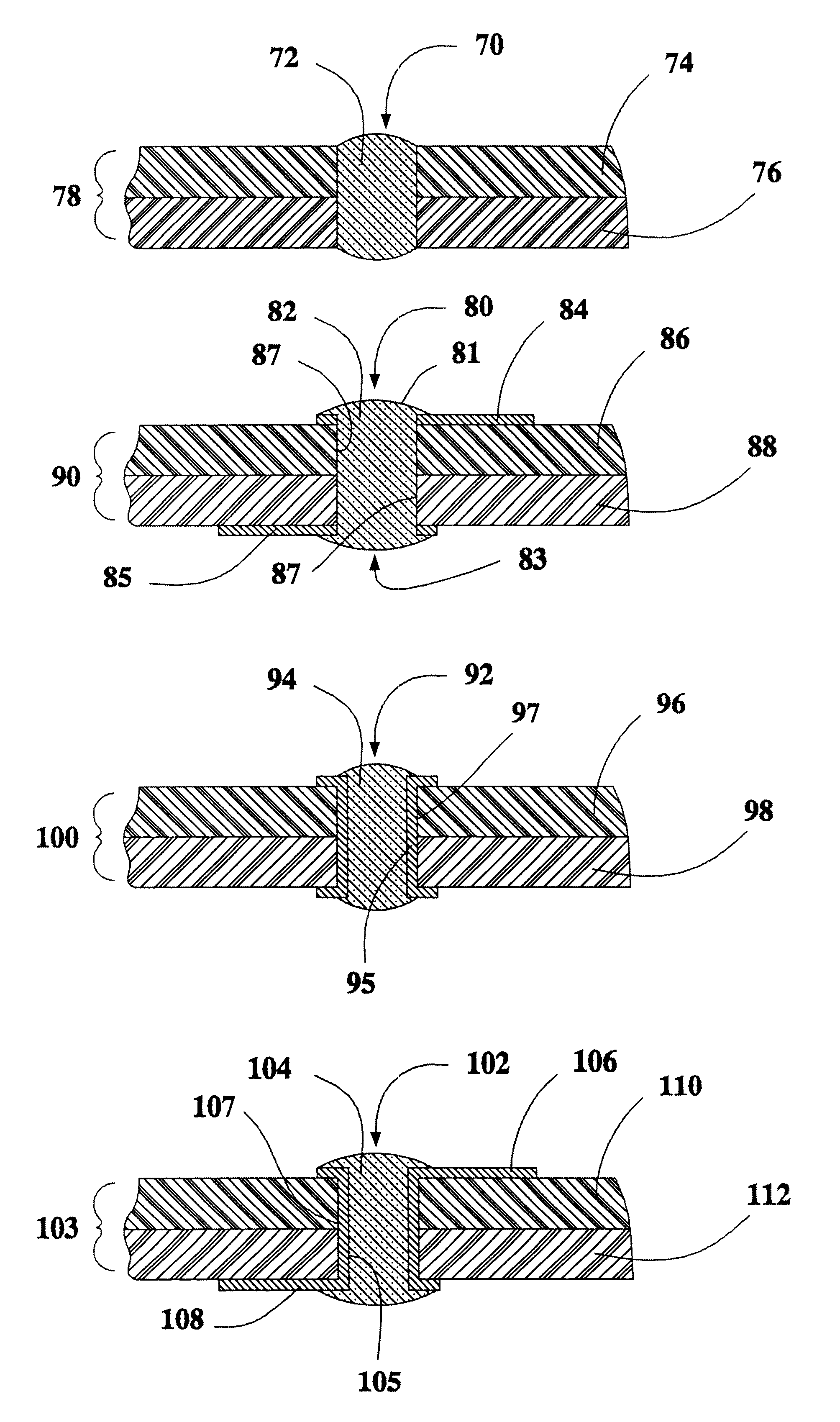
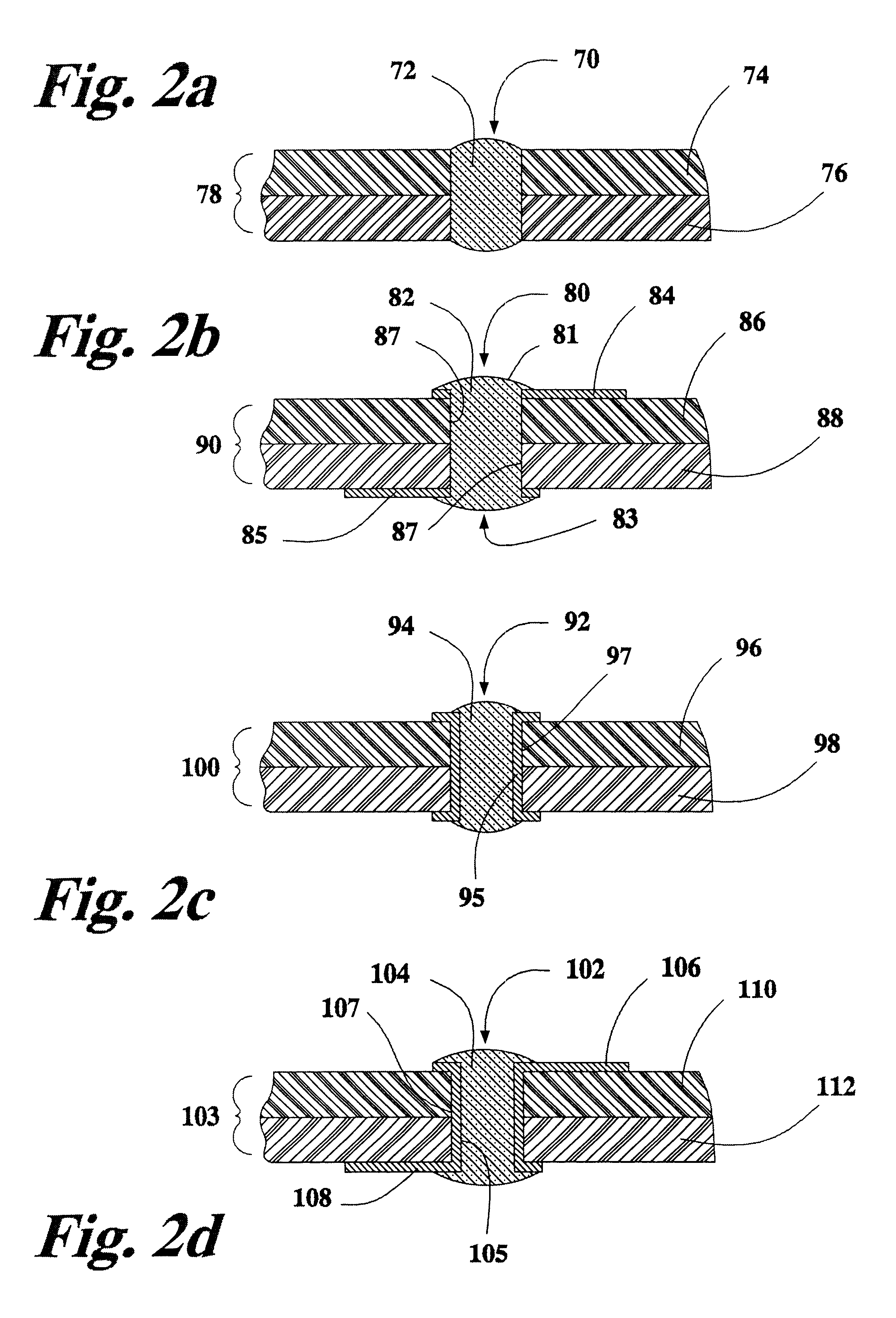
Printed wiring board conductive via hole filler having metal oxide reducing capability
a technology of metal oxide reduction and printed wiring, which is applied in the direction of printed element electric connection formation, non-metal conductors, conductors, etc., can solve the problems of affecting the electroplate performance of small diameter holes, affecting the electroplate quality of printed wiring boards, and requiring significant time for copper plating
- Summary
- Abstract
- Description
- Claims
- Application Information
AI Technical Summary
Benefits of technology
Problems solved by technology
Method used
Image

Examples
example 2
A composition was made as follows: 84 grams of Epon.RTM. 862 epoxy resin from Shell Oil Company was weighed into a container. To this was added 10 grams of Heloxy.RTM. CG-1400 from Air Products and Chemicals, Inc. After hand-stirring the mixture was passed through a 3-roll mill for further dispersion.
example 3
A composition was made as follows: 12 grams of paste from Example 1 were added to 4 grams of isophorone, 0.5 grams of LICA.RTM. 38, AND 83.5 grams of silver flake. After hand-stirring the mixture was passed through a 3-roll mill for further dispersion. A portion of a preoxidized copper sheet was covered with this paste and placed in an oven at 110 degrees Centigrade for 10 minutes. The paste was then removed to expose the surface of the copper underneath. It was found that the golden oxidation color was changed to a reddish color indicating some oxidation had been removed.
example 4
A composition was made as follows: 12 grams of paste from Example 2 were added to 4 grams of isophorone, 0.5 grams of LICA.RTM. 38, and 83.5 grams of silver flake. After hand-stirring, the mixture was passed through a 3-roll mill for further dispersion. A portion of a preoxidized copper sheet was covered with this paste and placed in an oven at 110 degrees Centigrade for 10 minutes. The paste was then removed to expose the surface of the copper underneath. It was found that the golden oxidation color was changed to a reddish color indicating some oxidation had been removed.
PUM
| Property | Measurement | Unit |
|---|---|---|
| distance | aaaaa | aaaaa |
| diameter | aaaaa | aaaaa |
| diameters | aaaaa | aaaaa |
Abstract
Description
Claims
Application Information