Method and apparatus for single crystal gallium nitride (GaN) bulk synthesis

a gallium nitride and bulk synthesis technology, applied in the field of material science, can solve the problems of two types of defects, heteroepitaxial growth, dislocation defects,

Inactive Publication Date: 2002-04-16
DOW CORNING CORP
View PDF7 Cites 72 Cited by
  • Summary
  • Abstract
  • Description
  • Claims
  • Application Information

AI Technical Summary

Problems solved by technology

However, heteroepitaxial growth has several technical drawbacks.
In particular, two types of defects arise as a result of heteroepitaxial growth: (i) dislocation defects due to lattice mismatch; and (ii) dislocation defects due to different thermal coefficients between the substrate and the epitaxial layer.
Many other substrates have been used, but all of them have large lattice mismatches and result in a high density of defects in the grown layers.
The second type of defect includes dislocations generated during cooldown after growth.
This defect is a result of different thermal coefficients of expansion of the substrate and epitaxial layer.
However, both suffer from deficiencies and / or limitations adversely affecting the quality of the GaN product.
While the buffer layers improve the crystallinity and surface morphology of the GaN compound semiconductor crystal, the crystal remains in a distorted state because of the lattice mismatch with the sapphire substrate.
This distorted state results in dislocation defects described herein.
One embodiment of this method uses aluminum garnet or gallium garnet as a substrate, but the lattice match using these compounds is not sufficient to provide much improvement.
Thermal decomposition of the substrate adversely affects the quality of the semiconductors obtained using this method.
As a result of these problems, typical GaN semiconductor devices suffer from poor device characteristics, short life span, and high cost.
Full utilization of the properties of GaN semiconductors cannot be realized until a suitable substrate is available that allows for growth of high quality homoepitaxial layers.
Uniform doping of typical GaN semiconductors having a non-GaN substrate is extremely difficult because the dopant has to be applied to the non-GaN substrate material.

Method used


Image

  • Method and apparatus for single crystal gallium nitride (GaN) bulk synthesis
  • Method and apparatus for single crystal gallium nitride (GaN) bulk synthesis
  • Method and apparatus for single crystal gallium nitride (GaN) bulk synthesis

Examples


Embodiment Construction

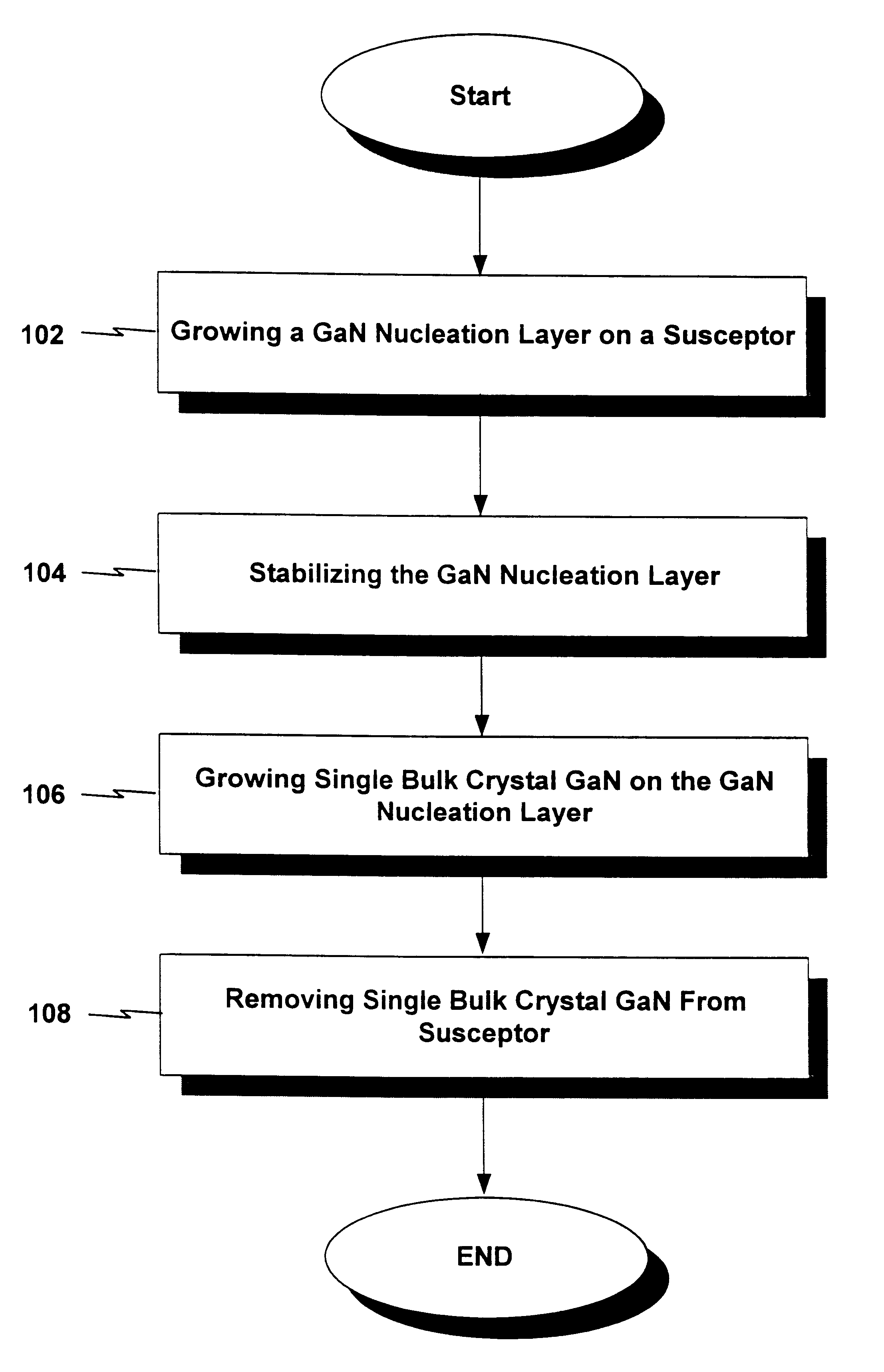
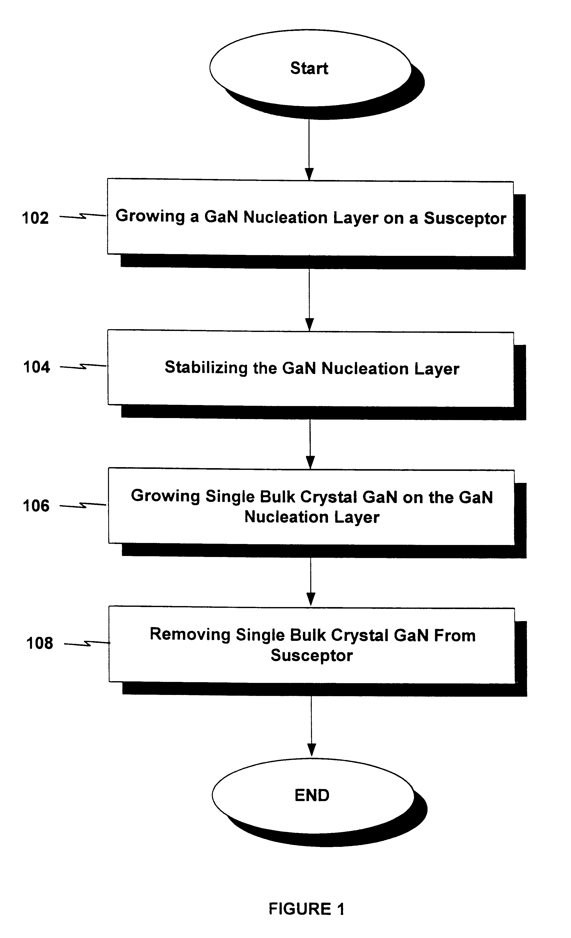
An experimental example of the production of the GaN single crystal includes a single crystal GaN grown by a three step process of creating a nucleation layer on a Pyro-Boron-Nitride susceptor, a second interconnection or stabilization step, and a third step of growing a GaN bulk layer on the nucleation layer. The Pyro-Boron-Nitride susceptor had a thickness of 3.5 to 4.5 mm, and it was cleaned with an organic solvent. The reactor chamber described herein was then evacuated to a pressure of 10.sup.-9 Torr. The temperature was then raised to a temperature in the range 300 to 800 degrees Celsius. The susceptor was rotated relative to the reactor chamber using a rotational velocity of 700 rpm. Chamber conditions were stabilized for ten minutes. The surface of the susceptor was cleaned by introducing 99.9999% pure Nitrogen (N.sub.2) gas at a pressure of 10.sup.-3 Torr. Nitrogen (N.sub.2) gas was provided at a flow rate of 5 to 10 cubic centimeters per minute; Ammonia (NH.sub.3) gas was ...


PUM

PropertyMeasurementUnit
temperatureaaaaaaaaaa
pressureaaaaaaaaaa

Abstract

A method and apparatus for homoepitaxial growth of freestanding, single bulk crystal Gallium Nitride (GaN) are provided, wherein a step of nucleating GaN in a reactor results in a GaN nucleation layer having a thickness of a few monolayers. The nucleation layer is stabilized, and a single bulk crystal GaN is grown from gas phase reactants on the GaN nucleation layer. The reactor is formed from ultra low oxygen stainless steel.

Description

1. Field of the InventionThis invention relates to the field of materials science and more particularly to the growth of semiconductor crystals.2. Description of the Related ArtThere is currently a demand in the computer and telecommunication industries for multicolor light emitting displays and improved data density in communication and recording. As a result of this demand, there is a strong desire for a semiconductor light emitting element capable of emitting light having shorter wavelengths ranging from a blue light wavelength to an ultraviolet wavelength.The III-V nitrides, as a consequence of their electronic and optical properties and heterostructure character, are highly advantageous for use in the fabrication of a wide range of microelectronic structures. In addition to their wide band gaps, the III-V nitrides also have direct band gaps and are able to form alloys which permit fabrication of well lattice-matched heterostructures. Consequently, devices made from the III-V ni...

Claims


Application Information

Patent Timeline
Patent Type & Authority Patents(United States)
IPC IPC(8): C30B25/00C30B25/02H01L21/205H01L21/02H01L33/00
CPCC30B25/00C30B25/02C30B29/406C30B29/60H01L21/02458H01L21/0262H01L21/0254H01L21/02389H01L33/0075C30B29/64
Inventor CHO, HAK DONGKANG, SANG KYU
Owner DOW CORNING CORP
Why Eureka
Try Eureka