Electric apparatus having a contact intermediary member and method for manufacturing the same

a technology of contact intermediary and electric equipment, which is applied in the direction of electrical equipment construction details, transportation and packaging, layered products, etc., can solve the problems of inability to say that the structure can sufficiently reduce the thermal resistance, and difficulty in reducing electrical resistan

Inactive Publication Date: 2002-04-30
DENSO CORP
View PDF25 Cites 55 Cited by
  • Summary
  • Abstract
  • Description
  • Claims
  • Application Information

AI Technical Summary

Problems solved by technology

However, since the oil or grease including the powder metal is an insulator as itself, it is difficult to sufficiently reduce the electrical resistance.
Furthermore, since these chemical synthetic materials have poor thermal conductivities compared to metal, it cannot say that this structure can sufficiently reduce the thermal resistance.
Hence, it also cannot say that this structure can sufficiently reduce the electric resistance between the main electrode surface of the semiconductor element and the electrode plate.
However, since a surface roughness of the soft metal foil is so small like a mirror surface, the contact intermediary member cannot fill up a small gap caused by an asperity of the main electrode surface of the semiconductor element or the surface of the electrode plate.
Therefore, it is difficult to sufficiently reduce, especially, the thermal resistance.
Here, physical damages include such as a load concentration due to a thermal distortion between the heat-emitting element and the electrode member during making the pressed-contact, or a wear of a contact surface (especially, the surface of the heat-emitting element) due to a difference in therm

Method used


Image

  • Electric apparatus having a contact intermediary member and method for manufacturing the same
  • Electric apparatus having a contact intermediary member and method for manufacturing the same
  • Electric apparatus having a contact intermediary member and method for manufacturing the same

Examples


fourth embodiment

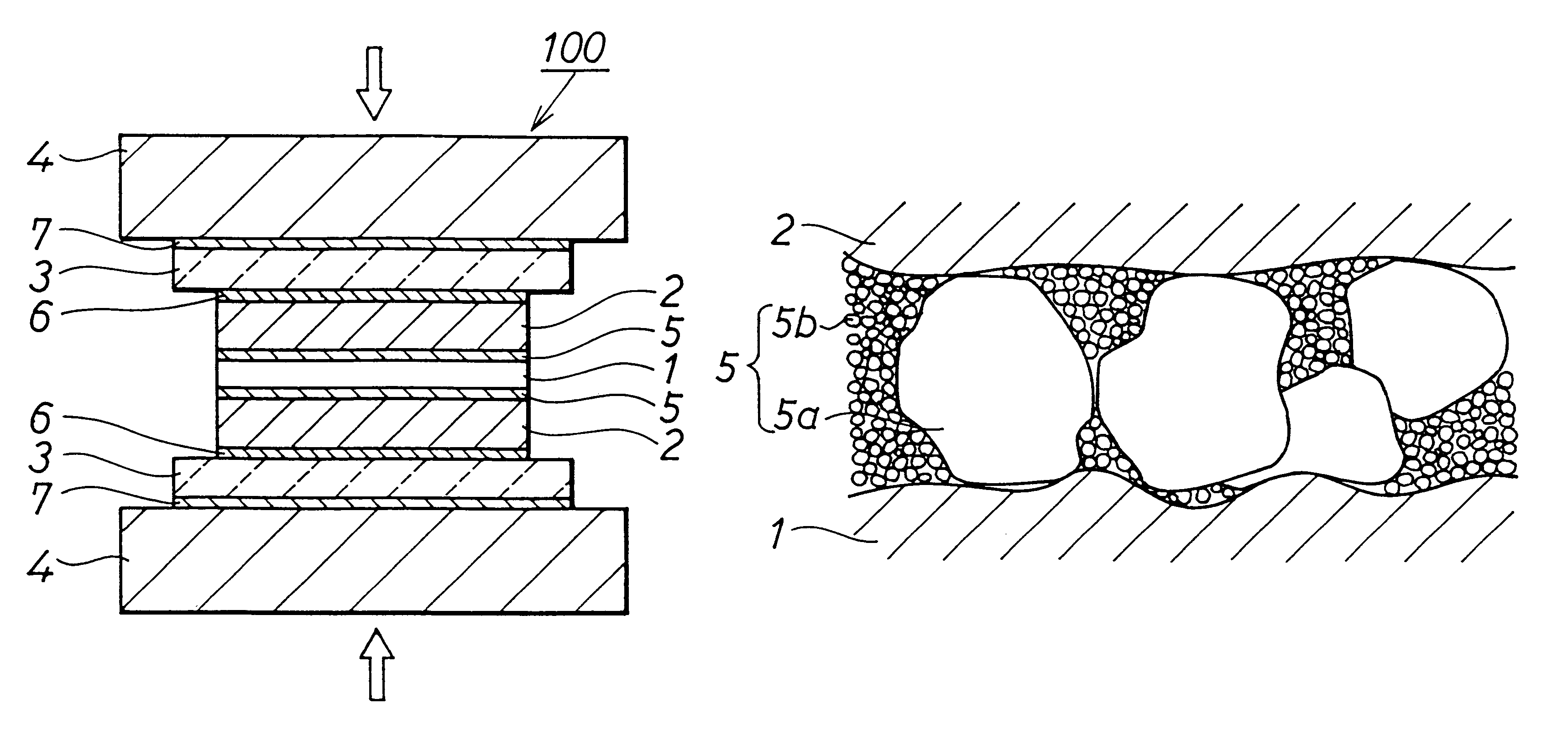
The fourth embodiment can be applied to a semiconductor device other than the pressed-contact type as shown in FIG. 7 as well as the pressed-contact type semiconductor device. Furthermore, it is acceptable to other semiconductor device in which the heat-emitting element is sandwiched by a pair of electrode members, which have both the thermal buffer function for buffering the heat from the heat-emitting element and the electrode function for taking out the electric signals from the heat-emitting element, and the electrode members are sandwiched by a pair of radiating member from the outer side.

fifth embodiment

[Fifth Embodiment]

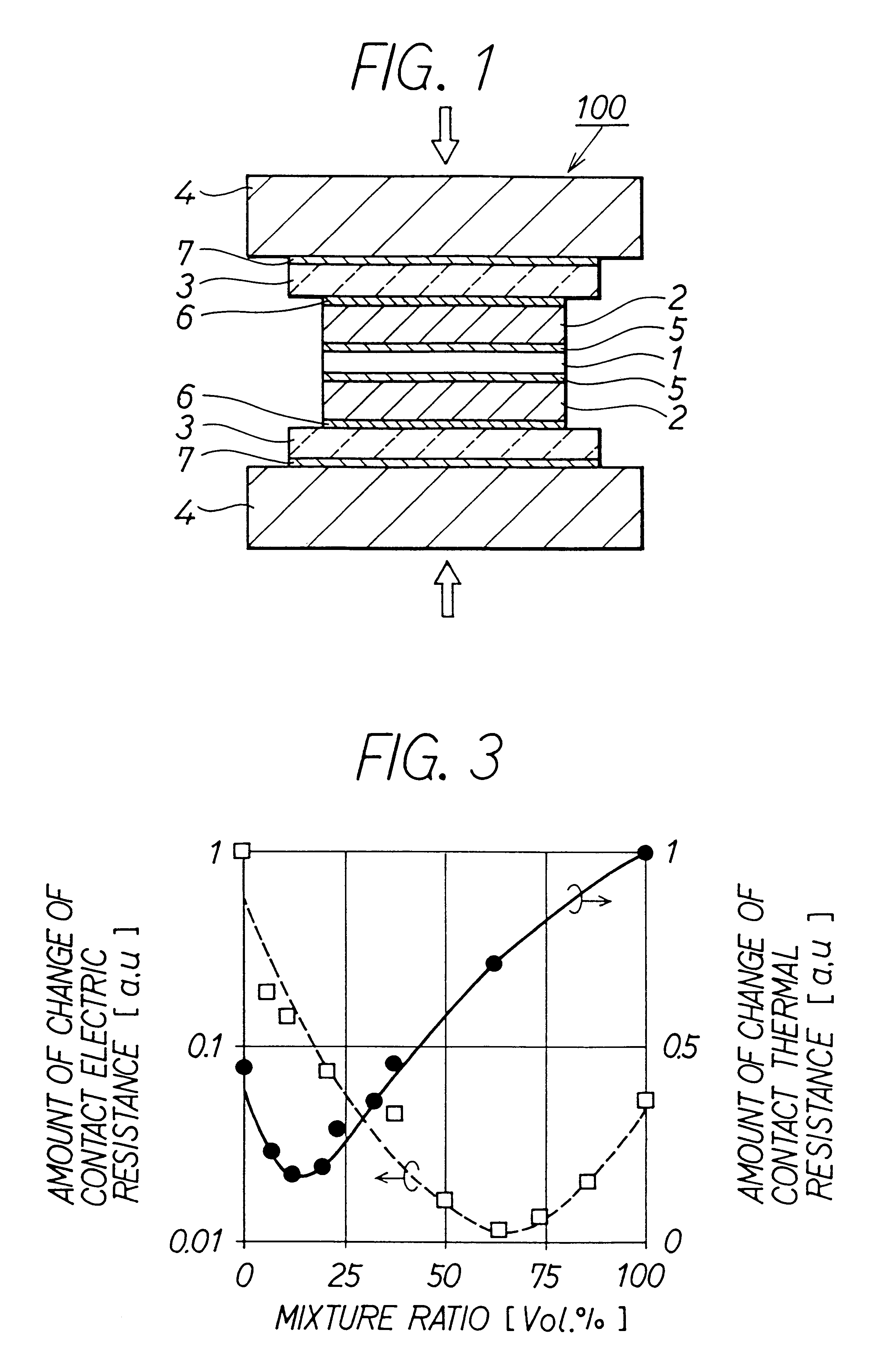
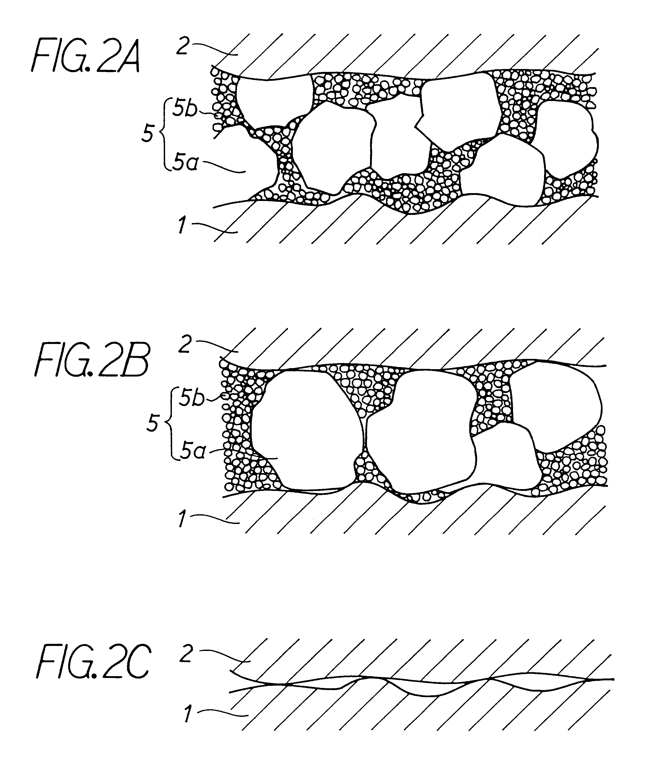
FIG. 9 is a schematic sectional view of a pressed-contact type semiconductor device 300 of a fifth embodiment according to the present invention. The pressed-contact type semiconductor device 300 is formed by adding a covering member 20 made of insulating material to the pressed-contact type semiconductor device 100 shown in FIG. 1.

In this embodiment, the covering member 20 is formed in a frame shape corresponding to an outer shape of the semiconductor element 1 and the electrode plate 2, and is provided so that an inner surface of the frame contacts with the outer peripheral surface of both the semiconductor element 1 and the electrode plate 2. Thus, the covering member 20 covers a surrounding portion of a region where the semiconductor element 1 contacts with the electrode plate 2 via the contact intermediary member 6 and a surrounding portion of a region where the electrode plate 2 contacts with the insulating plate 3 via the contact intermediary member 6. Here,...


PUM


Abstract

A pressed-contact type semiconductor device in which a main electrode surface of a semiconductor element is contacted with an electrode plate by a pressed-contact, which can reduce both an electric resistance and a thermal resistance between the main electrode surface of the semiconductor element and the electrode plate. The pressed-contact type semiconductor device (100) is provided with a semiconductor element (1) having electrode surfaces, a pair of electrode plates (2) contacted with the electrode surfaces by the pressed-contact, a pair of insulating plates (3) contacted with the outer side of the pair of the electrode plates by the pressed-contact, and a pair of radiating plates (4) contacted with the outer side of the pair of the insulating plates by the pressed-contact. A contact intermediary member (5), which is made up of particle member having at least thermal conductivity and electric conductivity, is intercalated between the semiconductor element and the electrode plate. The particle member of the contact intermediary member includes large particles 5a having an average particle diameter of more than 2 mum, and small particles 5b having an average particle diameter of to or less than 2 mum. Contact intermediary members (6, 7) are intercalated into gaps generated between the electrode plate and the insulating plate, and between the insulating plate and the radiating plate so as to fill up these gaps. The contact intemediary members are made of powder material having at least thermal conductivity.

Description

This application is based upon Japanese Patent Application Nos. Hei. 10-313982 filed on Nov. 9, 1998, Hei. 11-212731 filed on Jul. 27, 1999 and Hei. 11-264335 filed on Sep. 17, 1999, the contents of which are incorporated herein by reference.1. Field of the InventionThis invention relates to an electric apparatus, and particularly to an electric apparatus in which an electric signal from a heat-emitting element is output through an electrode member by contacting the heat-emitting element with the electrode member, and further particularly to an electric apparatus which can reduce an electric resistance and a thermal resistance between the heat-emitting element and the electrode member, and to a method of manufacturing the same.2. Related ArtThere has proposed a pressed-contact semiconductor device in which a main electrode surface of a semiconductor element (heat-emitting element) contacts with an electrode plate (electrode member) together by being externally pressed (hereinafter, ...

Claims


Application Information

Patent Timeline
IPC IPC(8): H01L23/48H01L23/40H01L21/52
CPCH01L24/72Y10T428/25H01L2924/01012H01L2924/01013H01L2924/01029H01L2924/01042H01L2924/01047H01L2924/01058H01L2924/01074H01L2924/01075H01L2924/01078H01L2924/01079H01L2924/01082H01L2924/01088H01L2924/09701H01L2924/13055H01L2924/19041H01L2924/19043H01L2924/30105H01L2924/01005H01L2924/01006H01L2924/01024H01L2924/01033H01L2924/1301H01L2924/01004H01L2924/1305Y10T428/251H01L2924/00
Inventor HIRAI, YASUYOSHINOMURA, KAZUHITOMAKINO, TOMOATSUYOSHIDA, TAKAHIKOSHIOZAWA, MASAHIROHASHIKAWA, ATSUSHIYORINAGA, MUNEO
Owner DENSO CORP
Why Eureka
Try Eureka