Conductive adhesive interconnection with insulating polymer carrier

a technology of conductive adhesive and polymer carrier, which is applied in the direction of printed circuit aspects, sustainable manufacturing/processing, final product manufacturing, etc., can solve the problems of reducing the ability of mechanical strain absorption, not alleviating the strain of cte mismatch, and not being compatible with electronic assemblies requiring or desiring the ability of component reworkability, etc., to achieve the effect of improving mechanical strain absorption and reliability

Inactive Publication Date: 2002-10-01
INVENSAS CORP
View PDF11 Cites 47 Cited by
  • Summary
  • Abstract
  • Description
  • Claims
  • Application Information

AI Technical Summary

Benefits of technology

is to provide electronic modules having solid conductive joints with enhanced mechanical strain absorption and reliability.
Another object of the invention is to provide improved surface mount technology for use in connecting smaller multi-chip modules having structural stability with greater strain absorption for a more reliable electronic assembly.
Still another object of the present invention is to provide an electronic component assembly or module having reducing silver migration.
It is another object of the present invention to provide a circuit board which provides reworkability between the joined substrates.
Yet another object of the present invention is to provide an electronic component assembly having reduced thermo-mechanical fatigue.

Problems solved by technology

However, as a result of the interposer comprising a thermoplastic polymer, the interposer is typically made of a high modulus non-compliant material which does not alleviate CTE mismatch induced strain through material movement.
However, such technology relies on strong, typically permanent, bonds between the interposer and both electronic components, and thereby is not compatible with electronic assemblies requiring or desiring the ability of component reworkability.
However, such soldering techniques produce solder bonds of very small height leading to decreased strain absorption capability, as well as costly high temperature reflows as a result of the double reflow operations.
However, these area array technologies are limited by strain absorption due to the allowable diameter of the solder sphere.
During normal operations, the entire module is subject to temperature excursions due to the functioning of the circuits on the chip, resistance heating of the solder joints, the wiring within the chip, and the wiring within the substrate.
This heating results in the expansion and contraction of all of these components as temperatures rise and fall.
This mismatch places stresses on the solder joints, and over time results in the fatigue of the solder joints.
Eventually, continual stress causes cracks to propagate completely across the solder joints leading to electrical failure of the electronic module.
Furthermore, CGA adds considerable cost, electrical properties are compromised, and manufacturing complexities are increased as a result of solder columns being easily bent during handling thus requiring special precautionary measures during processing.
However, it has been recognized that conductive adhesives are not as mechanically strong as solder joints causing failure under certain mechanical shock conditions when used as electrical interconnections.
Conductive adhesive bonds, which typically have a silver filler, are not a metallurgical bond as formed by the solder joints and thus are not as strong as the solder joint bond.
Further problems associated with conductive adhesive joints in electronic packaging include an increased contact resistance, oxidation of silver flakes, and silver migration may occur with temperature humidity and bias.
Also, the formation of metal oxide, hydroxide, and other corrosion byproducts at the interface between a conductive adhesive and the metal bonding surface may compromise both the electrical and mechanical stability of the adhesive bonds, and thus the performance and reliability of the resultant electronic assembly.
As prior art is directed to surface mount technology for connecting two components together to form an electronic assembly including the use of interposers, soldering techniques, and conductive adhesives, such techniques have their corresponding problems as discussed above.

Method used


Image

  • Conductive adhesive interconnection with insulating polymer carrier
  • Conductive adhesive interconnection with insulating polymer carrier
  • Conductive adhesive interconnection with insulating polymer carrier

Examples


Embodiment Construction

)

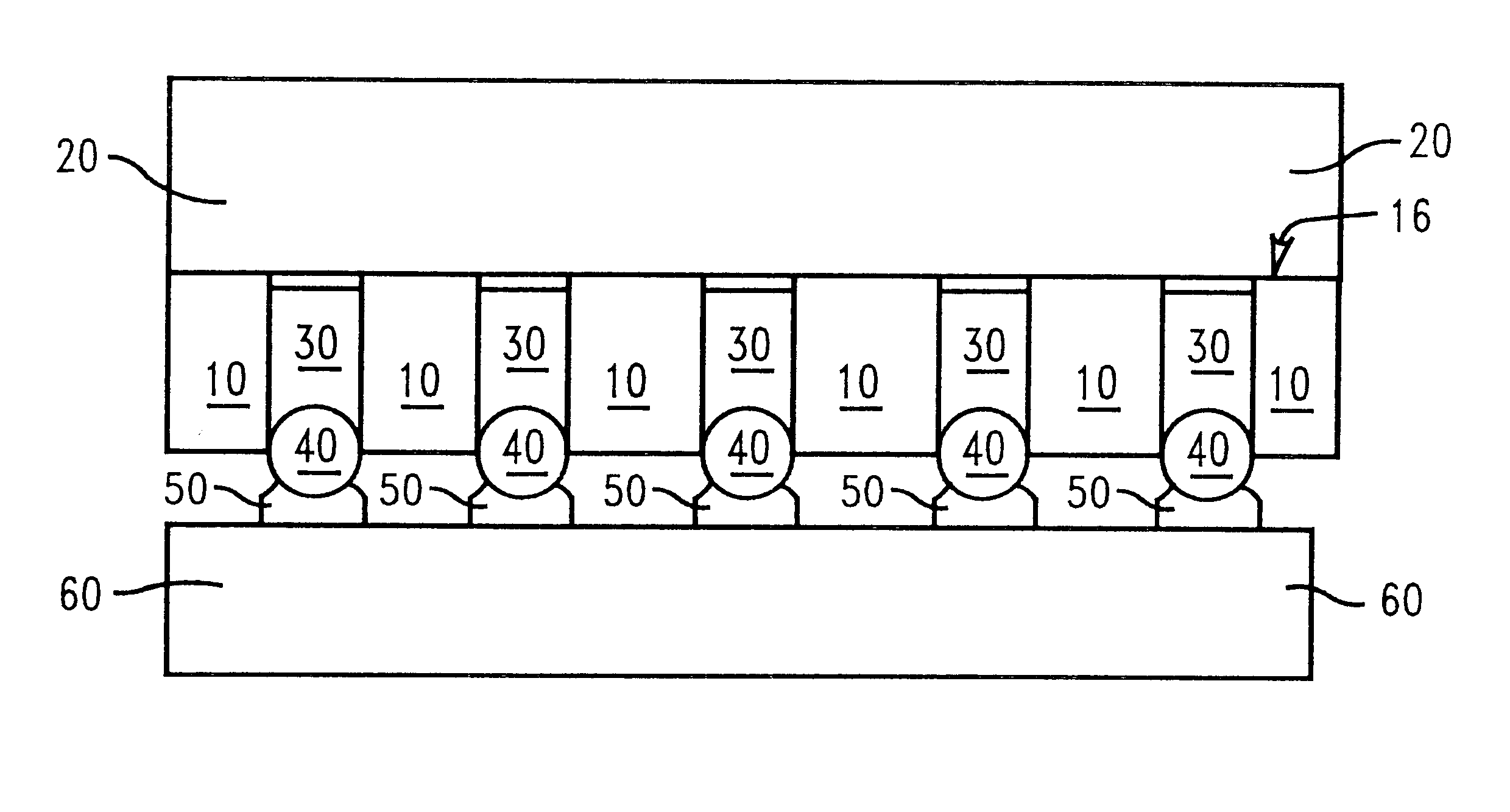
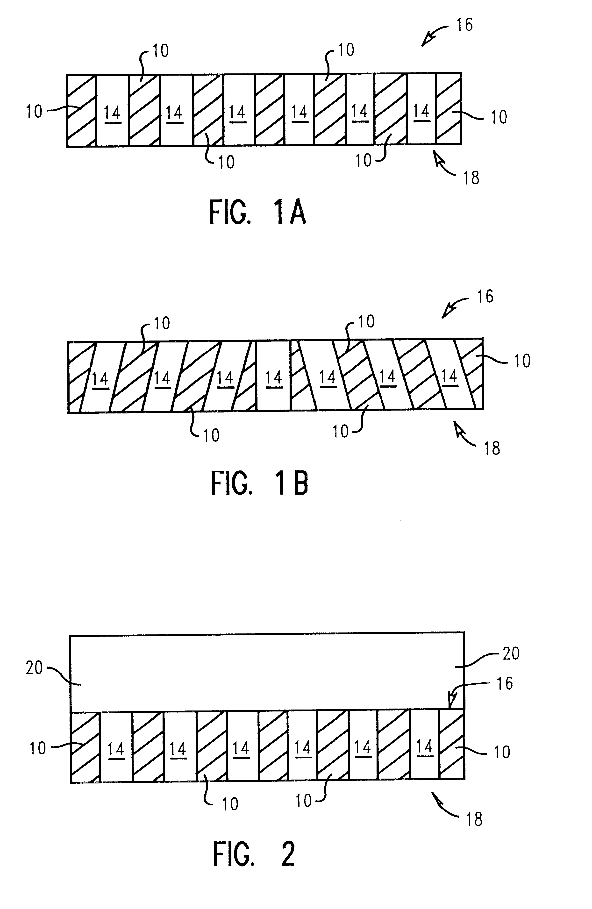
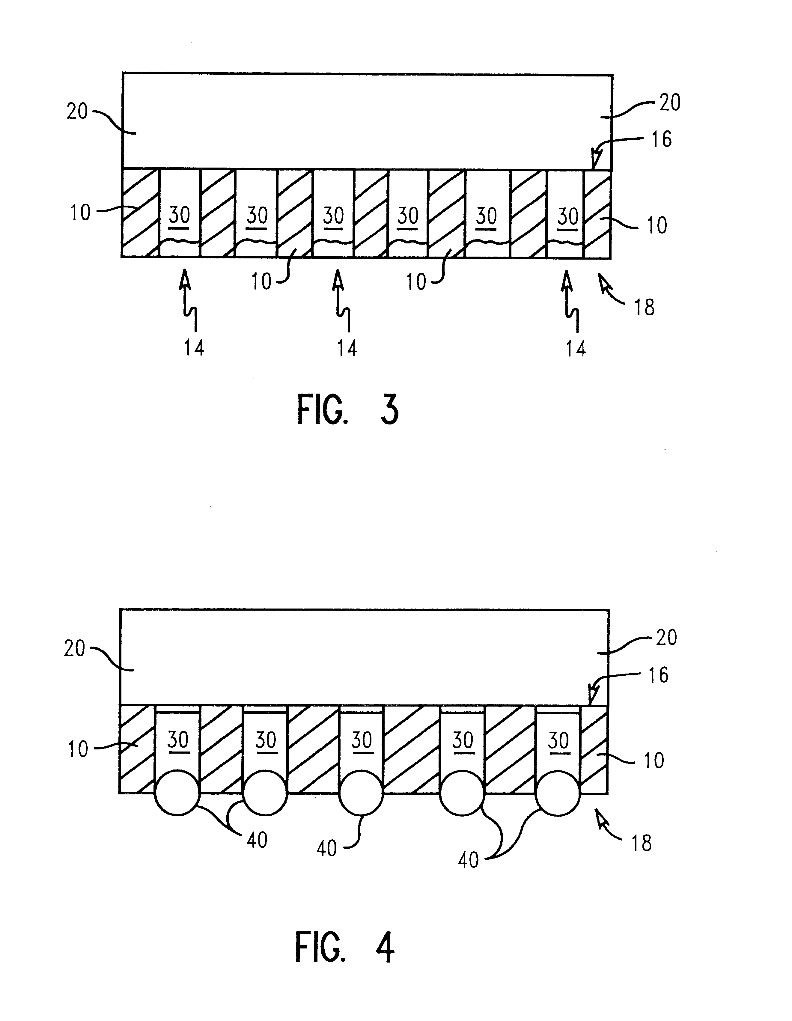
In describing the preferred embodiment of the present invention, reference will be made herein to FIGS. 1-6 of the drawings in which like numerals refer to like features of the invention. Features of the invention are not necessarily shown to scale in the drawings.

Manufacturers of printed circuit boards typically have to work with a selection of chip modules having different configurations of electrical connectors as well as different arrangements of the electrical connector footprints for connection to the corresponding contacts on the printed circuit boards. As used herein, the terms "contact arrangement" or "connector arrangement" refers to the pattern of the individual connectors or contacts, including the number and location of such contacts or connectors. As used herein, the term "contact configuration" or "connector configuration" refers to the type of physical and electrical connector utilized between the chip module and the printed circuit board, for example, pin grid arra...


PUM


Abstract

A method and apparatus is provided for forming an electronic assembly whereby an insulating polymer matrix having a plurality of conductor holes is attached to a first substrate wherein the conductor holes align with a corresponding contact array on the first substrate. Subsequently, a flexible, electrically conductive adhesive is provided within the plurality of conductor holes and a solid conductive material, preferably having a high melting temperature, is attached to at least one end thereof. The insulating polymer matrix with the electrically conductive adhesive and the solid conductive material is then cured at a temperature sufficient to completely cure the matrix to completely surround the electrically conductive adhesive, as well as permanently attaching the matrix and conductive adhesive to the first substrate and permanently attaching the solid conductive material to the conductive adhesive. A second substrate may then be attached to the conductive matrix structure secured to the first substrate by providing a low melting temperature attachment means to the solid conductive material attached to the matrix and subsequently reflowing the assembly to form an electronic assembly adapted with the capability of reworkability.

Description

1. Field of the InventionThe present invention relates to electronic assemblies, and in particular, to electrically and mechanically connecting two electronic components to form an electronic assembly having reduced thermo-mechanical fatigue, while also providing the electronic assembly with the ability to use existing bond and assembly technologies in addition to providing the assembly with reworkability.2. Description of Related ArtForming electronic assemblies by electrically connecting two components such as a multi-layer ceramic package or circuit chip to a card, board, or another connector is well known in the art. Such multi-layer electronic assembly formation is referred to in the art as surface mount technology which can include, but is not limited to, solder join, flip chip, C4, ball grid array and pin grid array. As will be recognized, surface mount technology has gained acceptance as the preferred means of joining electronic package assemblies, particularly in high end c...

Claims


Application Information

Patent Timeline
Patent Type & Authority Patents(United States)
IPC IPC(8): H01L21/60H01L21/02H01L23/48H01L23/498H05K3/34H05K3/32
CPCH05K3/3436H01L23/49827H01L24/81H01L24/83H01L24/29H05K2201/09472H05K2201/10992H05K2203/041H05K2203/0415H01L2224/13111H01L2224/81801H01L2224/8319H01L2224/838H01L2924/01005H01L2924/01029H01L2924/01047H01L2924/0105H01L2924/01051H01L2924/01079H01L2924/01082H01L2924/01322H01L2924/0781H01L2924/09701H01L2924/30107H05K3/321H01L2224/2919H01L2224/29298H01L2924/01006H01L2924/01033H01L2924/01087H01L2924/014H01L2924/0665H01L2224/29101H01L2924/0132H01L2924/0133H01L2224/29111H01L2924/00013H01L2924/07802H01L2924/00H01L2924/01083H01L2924/3512H01L2924/00014H01L2224/29099H01L2224/29199H01L2224/29299H01L2224/2929H01L2924/12042Y02P70/50
Inventor GOLDMANN, LEWIS S.INTERRANTE, MARIO J.JACKSON, RAYMOND A.OSTRANDER, AMY B.PERRY, CHARLES H.PETERSON, BRENDA L.
Owner INVENSAS CORP
Why Eureka
Try Eureka