Method and circuit for automatically correcting offset voltage

a technology of offset voltage and offset voltage, applied in the field of electric circuits, can solve the problems of limiting receiver sensitivity, inability to correct offset, piezoresistive changes in components, etc., and achieve the effect of robust offset correction

Inactive Publication Date: 2003-01-14
IBM CORP
View PDF1 Cites 41 Cited by
  • Summary
  • Abstract
  • Description
  • Claims
  • Application Information

AI Technical Summary

Benefits of technology

to provide a robust offset correction circuit which is inexpensive and requires no external measurement or correction programming.
These unique and unobvious features allow the claimed invention to correct offset voltages in high-gain differential amplifier chains in a manner which is robust, inexpensive and requires no external measurement or correction programming.

Problems solved by technology

However, when the gain on the incoming signal is too high, device mismatch in the differential transceivers creates an offset voltage which is amplified along with the signal of interest.
This offset voltage results in an error in determining the signal threshold at the analog-to-digital (A / D) converter and, if not corrected, will limit receiver sensitivity.
Transceivers may be produced without correcting offset voltage, in which case the transceivers will have to be examined after fabrication in a costly screening process to dispose of the modules which do not meet a required receiver sensitivity.
Further, the stresses induced on circuitry during packaging can cause piezoresistive changes in the components which can change the offset voltage.
Therefore, such offsets cannot be corrected until after packaging.
However, most modern digital complementary metal oxide semiconductor (CMOS) processes and analog BiCMOS processes cannot be laser trimmed because there are no laser trimmable resistors in the technology.
In addition, laser trimming adds expense and is a one-time operation with no possibility of "dynamic" trimming of offsets for changes in environmental conditions.
Unfortunately, this requires vastly greater die area and processing and, therefore, greater cost.
Additionally, in some circuits, the frequency content of the data is so varied that it is not possible to use such a dynamic, analog, continuous-time feedback loop.
Unfortunately, the charge on the capacitor which is used for offset correction slowly bleeds off due to inevitable leakage currents, and must be frequently refreshed.
In addition, this technique does not work in applications having no continuous, well-controlled clock reference, or in applications such as communications links which cannot tolerate signal chopping.
Unfortunately, neither of these methods provides a self-contained, inexpensive offset correction which requires no external measurement and correction programming.
Indeed, these techniques fail to address the need for offset correction in many analog applications which cannot be solved by feedback or chopper stabilization.

Method used


Image

  • Method and circuit for automatically correcting offset voltage
  • Method and circuit for automatically correcting offset voltage
  • Method and circuit for automatically correcting offset voltage

Examples


first embodiment

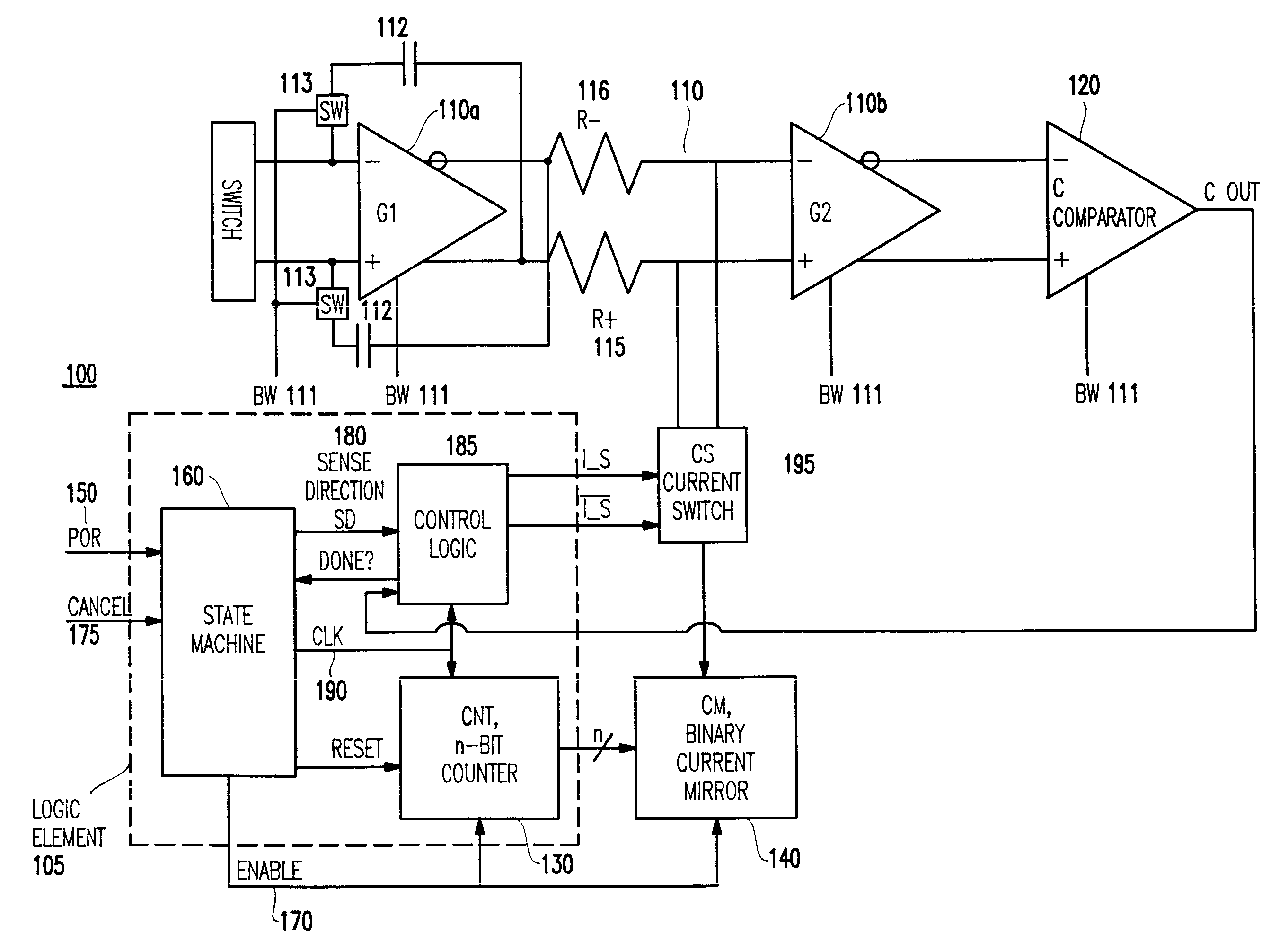
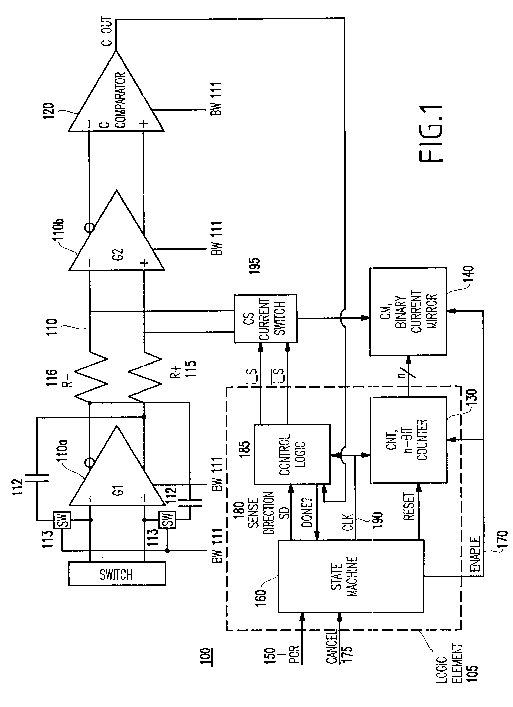
Referring now to the drawings, FIG. 1 shows an offset cancellation circuit 100 according to the present invention.

Generally, the offset correction circuit 100 according to the preferred embodiment includes a detector element (e.g., comparator 120) for detecting an offset voltage, a current switch 195, a current mirror 140 for generating an offset correction voltage, and a logic element 105. In the illustrative embodiment of FIG. 1, the offset correction circuit 100 is coupled to an amplifier chain 110 which includes a plurality of amplifiers G1 (110a), G2 (110b). Although the amplifier chain in FIG. 1 shows only two amplifiers it is clear to one of ordinary skill in the art that the amplifier chain may include any number of amplifiers.

Further, in FIG. 1, the detector element of the circuit is a comparator 120, although the detector element may also be an A / D converter. The comparator 120 is coupled to the output of the amplifier chain 110 and is used to sense the direction (or sign,...

second embodiment

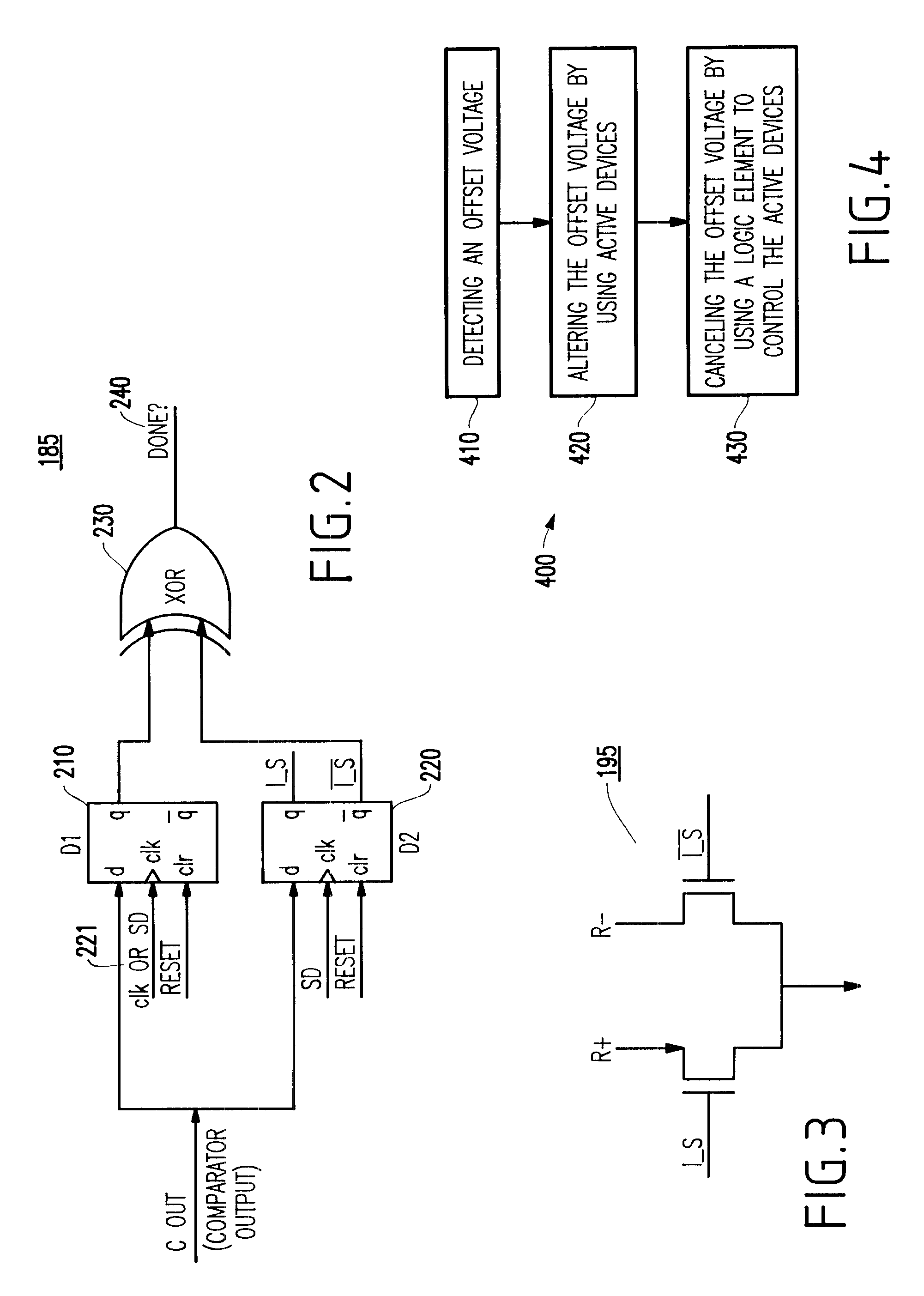
FIG. 4 illustrates a method for correcting an offset voltage in an amplifier chain 400 is provided according to the present invention. The method 400 includes a first detecting step 410 of the offset voltage. As explained above, this may be performed by a detector element which includes a comparator or an analog-to-digital converter.

In step 420, the offset voltage is altered by using active devices connected to an input of the amplifier chain. As explained above, this may be formed by a current mirror which generates an offset correction voltage and a current switch for directing the offset correction voltage into the amplifier chain.

Finally, in step 430, the offset voltage is canceled by using a logic element to control the active devices until the offset voltage is substantially canceled. Also as explained above, the logic element may include a self-contained state machine along with a control logic and counter.

These unique and unobvious features allow the claimed invention to cor...


PUM


Abstract

A circuit (and method) for correcting offset voltage in high-gain differential amplifier chains includes a detector element for detecting an offset voltage and a current mirror for generating an offset correction voltage. The circuit further has a current switch which outputs the offset correction voltage into the correct arm of the amplifier chain and a logic element which clocks the circuit, inputs a signal from the detector element and outputs a signal to the current switch.

Description

1. Field of the InventionThe present invention generally relates to an electrical circuit, and more specifically, to an electrical circuit used to automatically correct offset voltages in high-gain differential amplifier chains and which is robust, inexpensive and requires no external measurement or correction programming.2. Description of the Related ArtCommunications receivers, like infrared (IR) wireless receivers or radiofrequency (RF) wireless receivers, often require high gain to amplify incoming signals to usable amplitudes. Such receivers typically use differential transceivers to suppress common-mode noise generated by other circuitry on the same integrated circuit (IC).However, when the gain on the incoming signal is too high, device mismatch in the differential transceivers creates an offset voltage which is amplified along with the signal of interest. This offset voltage results in an error in determining the signal threshold at the analog-to-digital (A / D) converter and,...

Claims


Application Information

Patent Timeline
Patent Type & Authority Patents(United States)
IPC IPC(8): H03F3/45
CPCH03F3/45941
Inventor RITTER, MARK B.
Owner IBM CORP
Why Eureka
Try Eureka