

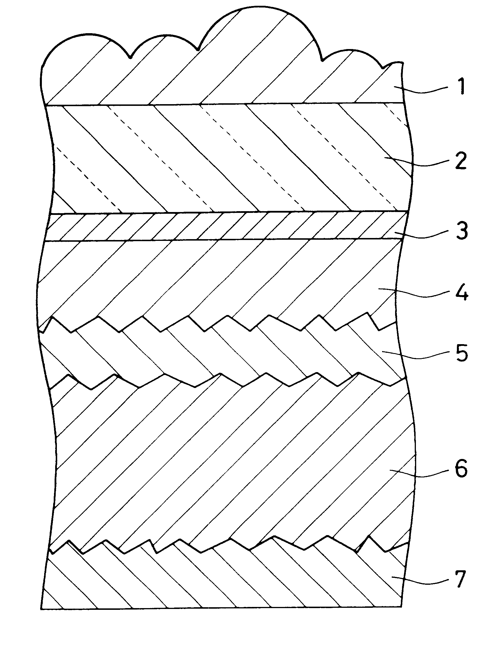
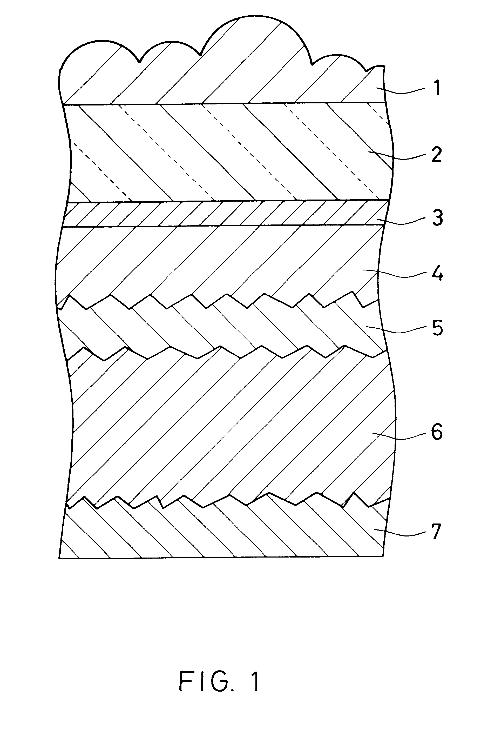
Photoelectric conversion device
a conversion device and photoelectric technology, applied in the direction of optical elements, pv power plants, instruments, etc., can solve the problems of degrading the quality of the crystalline silicon based thin film to be formed on the conventional photoelectric conversion device is not always provided with a structure suitable, and the quality of the transparent conductive film is not always suitable, so as to improve the photoelectric conversion efficiency of the photoelectric conversion layer, improve the photoelectric conversion efficiency, and reduce the cost of production
- Summary
- Abstract
- Description
- Claims
- Application Information
AI Technical Summary
Benefits of technology
Problems solved by technology
Method used
Image

Examples
Embodiment Construction
Hereinafter, the present invention will be described more specifically by way of example, but is not limited thereto.
Manufacture of Glass Sheet with Transparent Conductive Film
Sample 1
In a production line for float glass, a tin oxide film (SnO.sub.2 film), a silicon oxide film (SiO.sub.2 film), and a fluorine-containing tin oxide film (SnO.sub.2 :F film) were formed in this order on a glass ribbon using a plurality of coaters arranged in a float bath. The glass ribbon is formed to have a thickness of 4 mm and the total amount of iron oxide of 0.01 wt % in terms of Fe.sub.2 O.sub.3.
Specifically, the glass ribbon had a temperature of about 650.degree. C. immediately before reaching a coater located at the furthest upstream position, and a mixed gas of dimethyltin dichloride (vapor), oxygen and nitrogen was supplied from the coater, so that a SnO.sub.2 film having a thickness of 25 nm was formed on the glass ribbon. Then, a mixed gas of monosilane, ethylene, oxygen and nitrogen was sup...
PUM
| Property | Measurement | Unit |
|---|---|---|
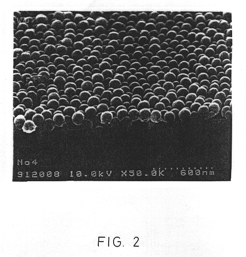
| particle diameter | aaaaa | aaaaa |
| light transmittance | aaaaa | aaaaa |
| band gap | aaaaa | aaaaa |
Abstract
Description
Claims
Application Information