Method of manufacturing multilayer wiring board

a manufacturing method and wiring board technology, applied in the direction of superimposed coating process, instruments, transportation and packaging, etc., can solve the problems of air becoming contaminant, difficult to fine-tune processing, limited size of via holes,

Inactive Publication Date: 2003-04-29
DENKA CO LTD
View PDF10 Cites 22 Cited by
  • Summary
  • Abstract
  • Description
  • Claims
  • Application Information

AI Technical Summary

Benefits of technology

According to the manufacturing method of the present invention, since the plating layer is formed not in the opening but on the whole surface and the pillar-like metallic body is formed by etching, laser emission or the like is not particularly required, and a diameter of the pillar-like metallic body can be reduced. Further, since the opening section from which the resist is removed is not plated, the reliability of conductivity between the lower wiring layer and the pillar-like metallic body is heightened. As a result, manufacturing can be carried out by simple facility and combination of conventional steps, and the multilayer wiring board, wherein the wiring layer can be thinned and the reliability of the wiring board is high, can be manufactured.
Another method of manufacturing a multilayer wiring board includes the step of forming a pillar-like metallic body on a topmost wiring layer by means of the above step of forming a pillar-like metallic body. Such a pillar-like metallic body is formed for mounting or the like of chip parts, but similarly to the case of the pillar-like metallic body between the wiring layers, the pillar-like metallic body having high density and reliability can be formed by simple facility and combination of conventional steps,

Problems solved by technology

However, as for the via hole, when the opening portion is formed and plated, there arises problems that fine processing is difficult and air becomes contaminant.
For this reason, in the case where reliability of the wiring board is maintained, the size of the via hole is limited.
Moreover, when multilayer are laminated, it is difficult to form a via hole just above a via hole, and the design of the laminated structure is restricted.
For this reason, the heightening of the density of the multilayer wiring boards is limited.
However, both the above methods have a problem that a height of the pillar-like conductor is easily non-uniform.
The former method has a problem that it takes a long time to form the pillar-like conductor because the electroless plating is carried out.
The latter method has a problem that current density cannot be heightened and similarly the formation of the pillar-like conductor takes a long time because the electrolytic plating is carried out.
Further, the formation of a resist pattern requires a large-scale apparatus for emitting a laser, and thus these methods are disadvantageous from the viewpoint of costs.
Further, since it is difficult to securely remove a resist on a bottom portion of the opening portion, reliability of conducting of the pillar-like conductor is lowered.
Moreover, since the patterned portion of the wiring layer is coated mainly with an insulator, a possibility of short circuit between patterns is small, and the reliability becomes high and thinning is possible.
On the contrary, when an erosion amount is too small, the plating layer 24 remains on the non-pattered portion thereby to occasionally cause short-circuit.

Method used


Image

  • Method of manufacturing multilayer wiring board
  • Method of manufacturing multilayer wiring board
  • Method of manufacturing multilayer wiring board

Examples


second embodiment

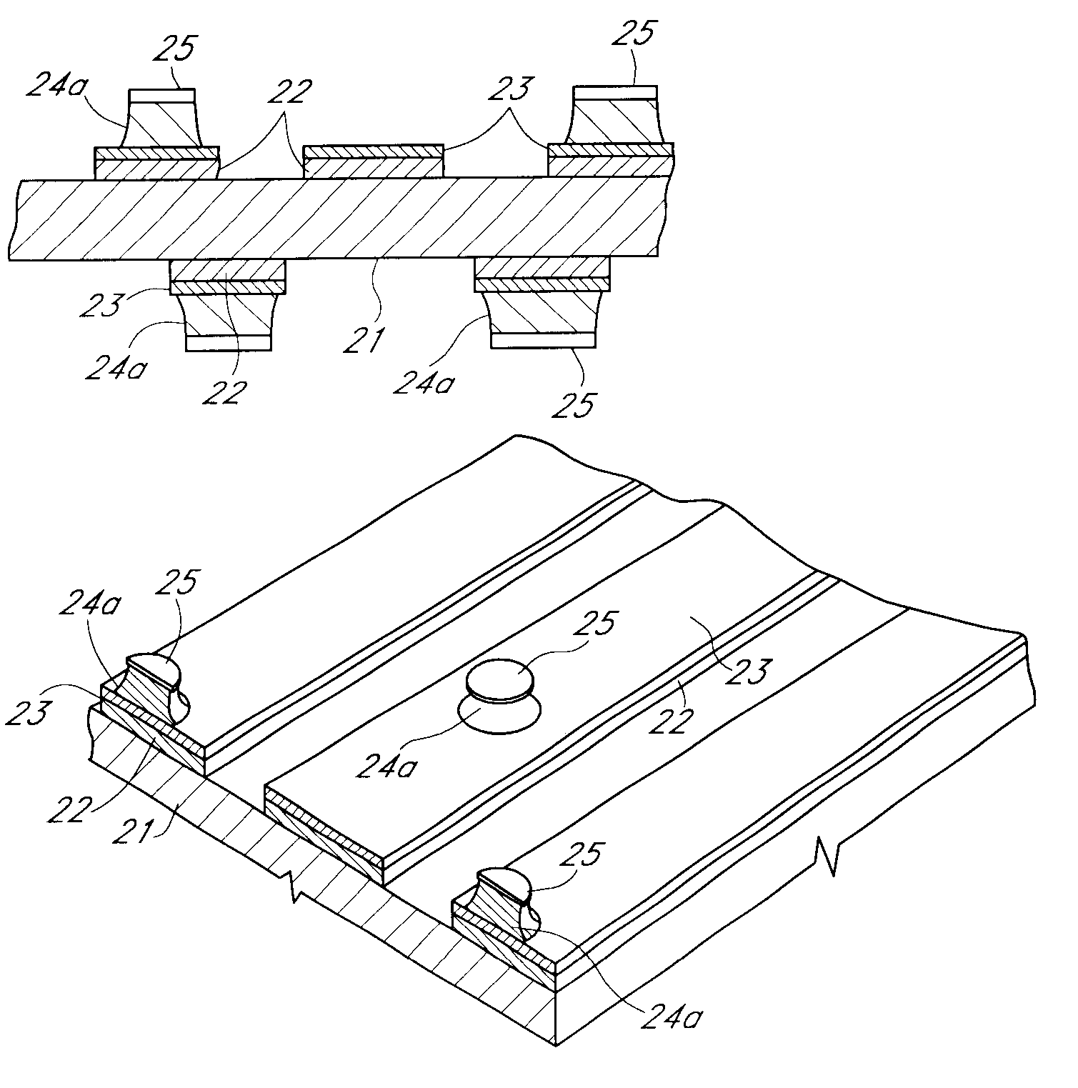
The present embodiment explains an example that a wiring layer and a pillar-like metallic body are formed on both the surfaces of the substrate as an insulating layer.

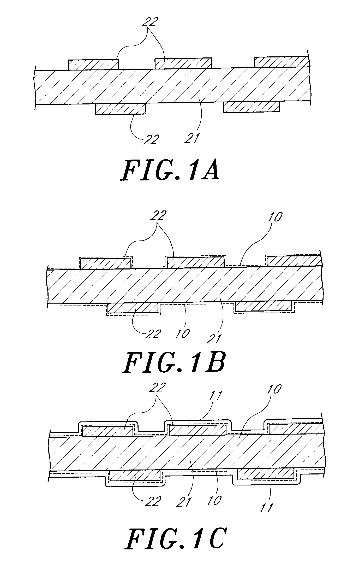
At first, as shown in FIG. 4a, a substrate 21 as an insulating layer where a metallic panel layer 22a is formed on its approximately whole surface is prepared. As the substrate 21, a substrate which is made of, for example glass fiber and various reactive curing resin such as epoxy resin and polyimide resin can be used. Moreover, as the metal constituting the metallic panel layer 22a, normally copper, nickel, tin or the like is used, and preferably copper is used. The metallic panel layer 22a can be formed by laminating by means of plating, adhesive, thermocompression bonding or the like. In the case where plating is carried out, electroless plating, or a combination of electroless plating and electrolytic plating can be adopted.

As shown in FIG. 4b, at step (2a), a conductive layer 23, which has resistance at the time ...

third embodiment

The present embodiment describes the example that when the wiring layer is laminated an both the surfaces of the substrate, the pillar-like metallic body is formed on both the surfaces of the substrate.

At first, as shown in FIG. 5a, the substrate 21 where the wiring layer 22 is patterned on its both surfaces is prepared. At this time, any patterning method may be used, and for example, a method using etching resist, a method using pattern plating resist or the like may be used. As the substrate 21, a substrate composed of glass fiber and various reactive curing resin such as polyimide resin and the like can be used, and as the metal constituting the wiring layer 22, normally copper, nickel tin or the like is used.

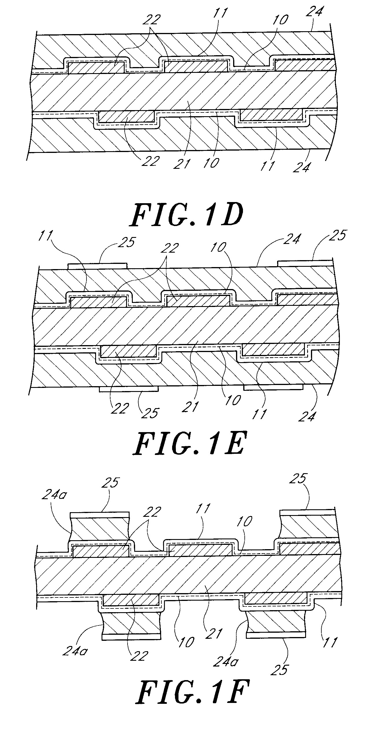
At step (3a), as shown in FIGS. 5b through 11 (4), a protective layer, in which a portion where the pillar-like metallic body 24a is formed is formed by the conductor 23, and the other portion is formed by a insulator 20b, is formed so as to cover the approximately whole su...


PUM

PropertyMeasurementUnit
thicknessaaaaaaaaaa
thicknessaaaaaaaaaa
outer diameteraaaaaaaaaa

Abstract

A method of manufacturing a multilayer wiring board comprising a step of forming an upper wiring layer (27), a part thereof being electrically connected to a pillar-shaped metallic body (24a), after he pillar-shaped metal body (24a) is formed on a lower wiring layer (22) is characterized in that the step of forming the metallic body includes a sub-step of forming a plating layer (24) constituting the metallic body, a sub-step of forming a mask layer (25) on the surface where the metal body is formed, of the plating layer, and a sub-step of etching the plating layer. The manufacture can be carried out with simple equipment combination of conventional steps and the wiring layer can be made fine. Moreover, a multilayer wiring board having a high reliability can be manufactured,

Description

1. Field of the InventionThe present invention relates to a multilayer wiring board having two or more wiring layers and a manufacturing method thereof. More specifically, this invention relates to the multilayer wiring board and the manufacturing method thereof having the step of forming an upper wiring layer, a part thereof being electrically connected with a pillar-like metallic body, after the pillar-like metallic body is formed on a lower wiring layer.2. Description of the Related ArtIn recent years, as electronic equipiments and the like are miniaturized and light-weighted, electronic parts are miniaturized and wiring boards onto which the electronic parts are mounted are required to be higher density, In order to heighten the density of the wiring boards, a method of heightening line density of wiring layers or a method of obtaining a multilayer structure by laminating a plurality of wiring layers are adopted.The method of manufacturing a multilayer wiring board includes a jo...

Claims


Application Information

Patent Timeline
Patent Type & Authority Patents(United States)
IPC IPC(8): H05K3/46
CPCH05K3/4647H05K2203/0384Y10T428/24917H05K2203/0733H05K2203/0542H05K3/46B32B3/00
Inventor YOSHIMURA, EIJIHIGUCHI
Owner DENKA CO LTD
Why Eureka
Try Eureka