Low power low noise amplifier

a low-noise amplifier and low-power technology, applied in the direction of amplifier combinations, low-noise amplifiers, gain control, etc., can solve the problems of difficult to obtain high-power linearity and power gain in low-power rf receivers, and achieve the effect of improving linearity and low power consumption

Inactive Publication Date: 2003-04-29
KOREA ADVANCED INST OF SCI & TECH
View PDF4 Cites 39 Cited by
  • Summary
  • Abstract
  • Description
  • Claims
  • Application Information

AI Technical Summary

Benefits of technology

So, the present invention contrived to solve the above mentioned problem is proposed to improve linearity and to obtain high power gain with low power.
The present invention is characterized by having a structure that improves linearity with low power consumption by using a third order intermodulation component with the parallel-connected common source transistor and common gate transistor.

Problems solved by technology

However, in the conventional amplifier structure, high power gain cannot be obtained due to low transconductance when the amplifier is operated with low power using low bias current.
Therefore, it is difficult to obtain high enough linearity and power gain in an RF receiver with low power.

Method used


Image

  • Low power low noise amplifier
  • Low power low noise amplifier
  • Low power low noise amplifier

Examples


first embodiment

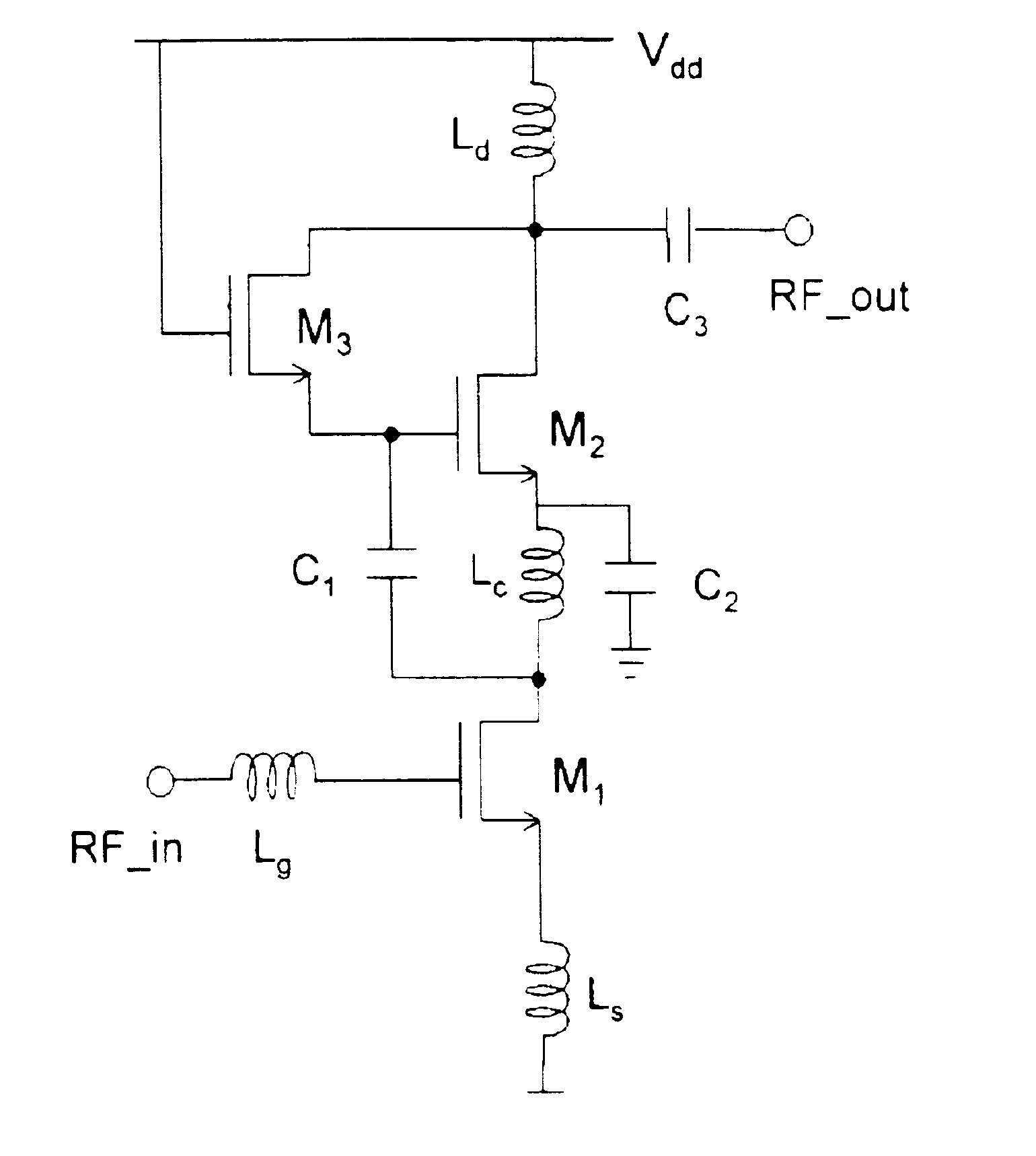
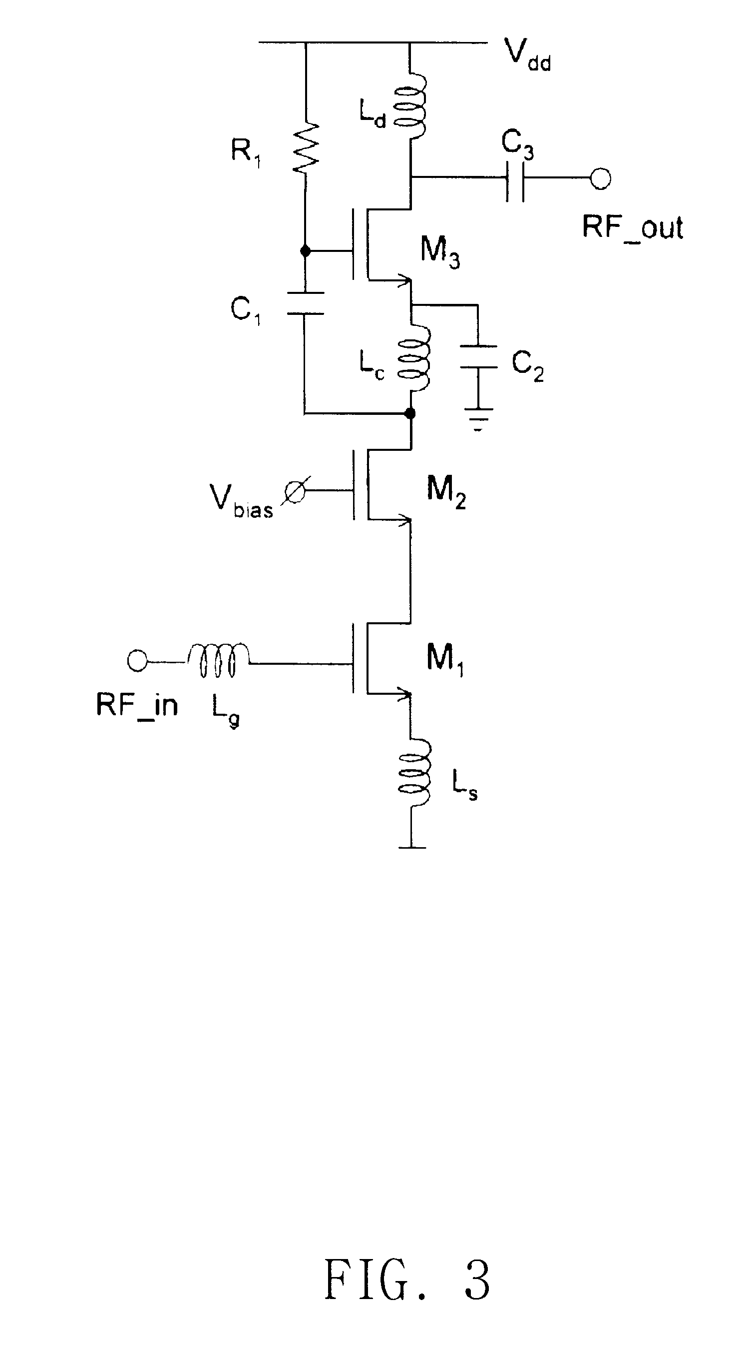
FIG. 3 is the present invention.

Herein, inductors L.sub.g and L.sub.s are used for matching input impedance, and inductor L.sub.d and capacitor C.sub.3 are used for matching output impedance.

Herein, the capacitor C.sub.2 is a bypass capacitor. So, source of common source component transistor M.sub.3 is bypassed by the C.sub.2.

In this structure, the signal amplified as much the gain by cascode structure composed of transistors M.sub.1 and M.sub.2 is amplified through coupling to the gate of common source transistor M.sub.3 by capacitor C.sub.1.

The entire gain is obtained by multiplying of the gain of cascode amplifier and common source amplifier. Therefore, the high power gain can be obtained compared to the conventional common source amplifier or cascode amplifier.

Herein, transistors M.sub.1 and M.sub.2 are operated as cascode amplifier, and transistor M.sub.3 is used as common source amplifier, and there is no increase of the bias current because the bias current is shared. Therefo...

second embodiment

FIG. 4 is the present invention.

In this structure, the signal amplified by common source component transistor M.sub.1 is coupled to gate of transistor M.sub.2 by capacitor C.sub.1 and is output after being amplified as much as the gain by the cascode structure composed of the said transistors M.sub.1 and M.sub.2.

Herein, transistor M.sub.1 is operated as a common source amplifier, and transistors M.sub.2 and M.sub.3 are operated as a cascode amplifier, and because the bias current is shared, there is no increase of the bias current. In this case, source of transistor M.sub.2 is bypassed by capacitor C.sub.2.

The entire gain is obtained by multiplying of the gain of cascode amplifier and common source amplifier. Therefore, the high power gain can be obtained compared to the conventional common source amplifier or cascode amplifier.

third embodiment

FIG. 5 is the present invention.

In this structure, the signal amplified by transistor M.sub.1 is coupled by N-type transistors M.sub.2 and P-type transistor M.sub.3 and then is output.

This structure gives higher power gain by sharing the bias current compared to the conventional structure and compensates linearity got worse in the high power gain structure.

The inverter type amplifier unit composed of transistors M.sub.2 and M.sub.3 have good linearity by push-pull operating, and it increases the linearity of the entire low noise amplifier.

Also, by sharing the bias current, higher power gain can be obtained with low current compared to the conventional common source amplifier or inverter type amplifier.


PUM


Abstract

A low power low noise amplifier achieves a high power gain without increasing power consumption by sharing the bias current. The amplifier is composed of a cascade structure which consists of a parallel connected common source transistor and common gate transistor connected to a common source transistor, an inverter type structure connected to the common source transistor, and structure improving the third-order intermodulation component using the parallel connected common source transistor and common gate transistor.

Description

1. Field of the InventionThe present invention related to a low power low noise amplifier, more particularly to the low power low noise amplifier which gives high power gain with low power consumption by improving the conventional low noise amplifier.2. Description of the Related ArtA low noise amplifier (LNA), which is used for RF receiver in a wireless communication application, is used necessarily at a receiver for obtaining power gain and decreasing noise factor (NF).A RF system in a wireless communication application requires a low power structure especially for portable communication system. Therefore, it should be designed to be consumed the least power within the range which can be satisfied in.However, the conventional low noise amplifier needs high power consumption at the RF receiver to satisfy the required power gain and characteristics compared to the present invention. The conventional LNA uses one unit common source amplifier structure showing as FIG. 1 or cascode amp...

Claims


Application Information

Patent Timeline
Patent Type & Authority Patents(United States)
IPC IPC(8): H03F1/08H03F1/22H03F1/26H03F3/193
CPCH03F1/223H03F3/193H03F2200/372H03F2200/294H03F2200/168H03F1/26
Inventor KWON, ICK JINGIL, JOON HOSHIN, HYUNG CHEOL
Owner KOREA ADVANCED INST OF SCI & TECH
Why Eureka
Try Eureka