Compound semiconductor laser

a semiconductor laser and compound technology, applied in semiconductor lasers, laser details, nanotechnology, etc., can solve the problems of less precise technique, large damage to the controllability of the transverse mode, and difficult to fabricate a semiconductor laser with a uniform transverse characteristic with a high yield, so as to improve the production yield of the laser, control the transverse mode stable, and the error tolerance range of etching large

Inactive Publication Date: 2003-07-22
SHARP KK
View PDF9 Cites 39 Cited by
  • Summary
  • Abstract
  • Description
  • Claims
  • Application Information

AI Technical Summary

Benefits of technology

The present invention enables to provide a device structure in which a transverse mode does not vary against a variation of the amount of etching, and to efficiently fabricate a ridge waveguide type III group nitride semiconductor laser with uniform characteristics.
Furthermore, by employing InGaAlN as a material for a semiconductor layer deposited on the second cladding layer, which exhibits a lower refractive index than that of the second cladding layer, respective III group nitride layers which are sequentially grown on the layer can be epitaxially grown while suppressing the generation of a defect, thereby improving the reliability of the laser.

Problems solved by technology

However, in the conventional ridge waveguide type III group nitride semiconductor laser as shown in FIG. 1, there was a problem that fabricating a semiconductor laser having a uniform transverse characteristic with a high yield is extremely difficult.
However, time control or else employ a less precise technique.
As a result, a film thickness of the P--AlGaN layer 210 varies between plural lots or in the same wafer, whereby controllability of the transverse mode is considerably damaged, and the production yield deteriorates.
Another problem is short lifetime under the CW condition at a room temperature.
More specifically, the above problem results from side surfaces and a bottom surface of a semiconductor to be etched being damaged by an etching treatment, thereby causing a crystal defect, and pinholes being present in SiO.sub.2 of an SiO.sub.2 protection film covering a p-AlGaN cladding layer on the side surface of the ridge and outside the ridge, whereby the crystal surface in fact cannot be sufficiently protected.

Method used


Image

  • Compound semiconductor laser
  • Compound semiconductor laser
  • Compound semiconductor laser

Examples


example 2

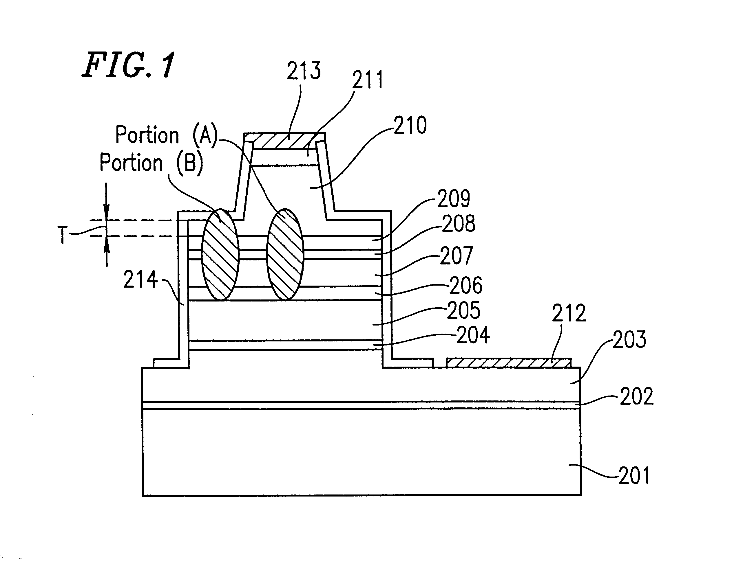
FIG. 8 is a schematic view showing a cross-sectional structure of a semiconductor laser according to Example 2 of the present invention. The laser diode of the present invention uses an insulating substrate. A fabrication process thereof has fabrication steps substantially identical with those of Example 1.

First, an undoped GaN buffer layer 402 of 20 nm, an n-GaN contact layer 403 of 5 .mu.m, an n-Al.sub.0.08 Ga.sub.0.92 N first cladding layer 404 of 1 .mu.m, an n-GaN light confining layer 405 of 0.1 .mu.m, an active layer 406 of InGaN-MQW structure, a p-Al.sub.0.2 Ga.sub.0.8 N evaporation preventing layer 407 of 0.05 .mu.m, a p-GaN light confining layer 408 of 0.1 .mu.m, a p-AlGaN second cladding layer 409 of 0.2 .mu.m, a p-GaN light guiding layer 410 of 0.05 .mu.m, a p-Al.sub.0.08 Ga.sub.0.92 N third cladding layer 411 of 0.8 .mu.m, and a p-GaN contact layer 412 of 0.5 .mu.m are epitaxially grown on a sapphire substrate 401 having a (0001) plane orientation (plane C) in a sequenti...

example 3

FIG. 9 is a schematic view showing a cross-sectional structure of a semiconductor laser according to Example 3 of the present invention. A laser diode of the present example is fabricated according to a process as follows.

First, an undoped GaN buffer layer 502 of 20 nm, an n-Al.sub.0.08 Ga.sub.0.92 N first cladding layer 503 of 1 .mu.m, an n-GaN light confining layer 504 of 0.1 .mu.m, an active layer 505 having an InGaN-MQW structure, a p-Al.sub.0.2 Ga.sub.0.8 N evaporation preventing layer 506 of 0.05 .mu.m, a p-GaN light confining layer 507 of 0.1 .mu.m, and a p-Al.sub.0.08 Ga.sub.0.92 N second cladding layer 508 of 0.2 .mu.m, a p-Al.sub.0.02 Ga.sub.0.98 N light guiding layer 509 of 0.05 .mu.m, a p-Al.sub.0.08 Ga.sub.0.92 N third cladding layer 510 of 0.8 .mu.m, and a p-GaN contact layer 511 of 0.5 .mu.m are epitaxially grown on an n-SiC substrate 501 in a sequential manner by the MOCVD method.

Next, a mask is applied to a portion of the p-contact layer 511, and an unmasked portion...
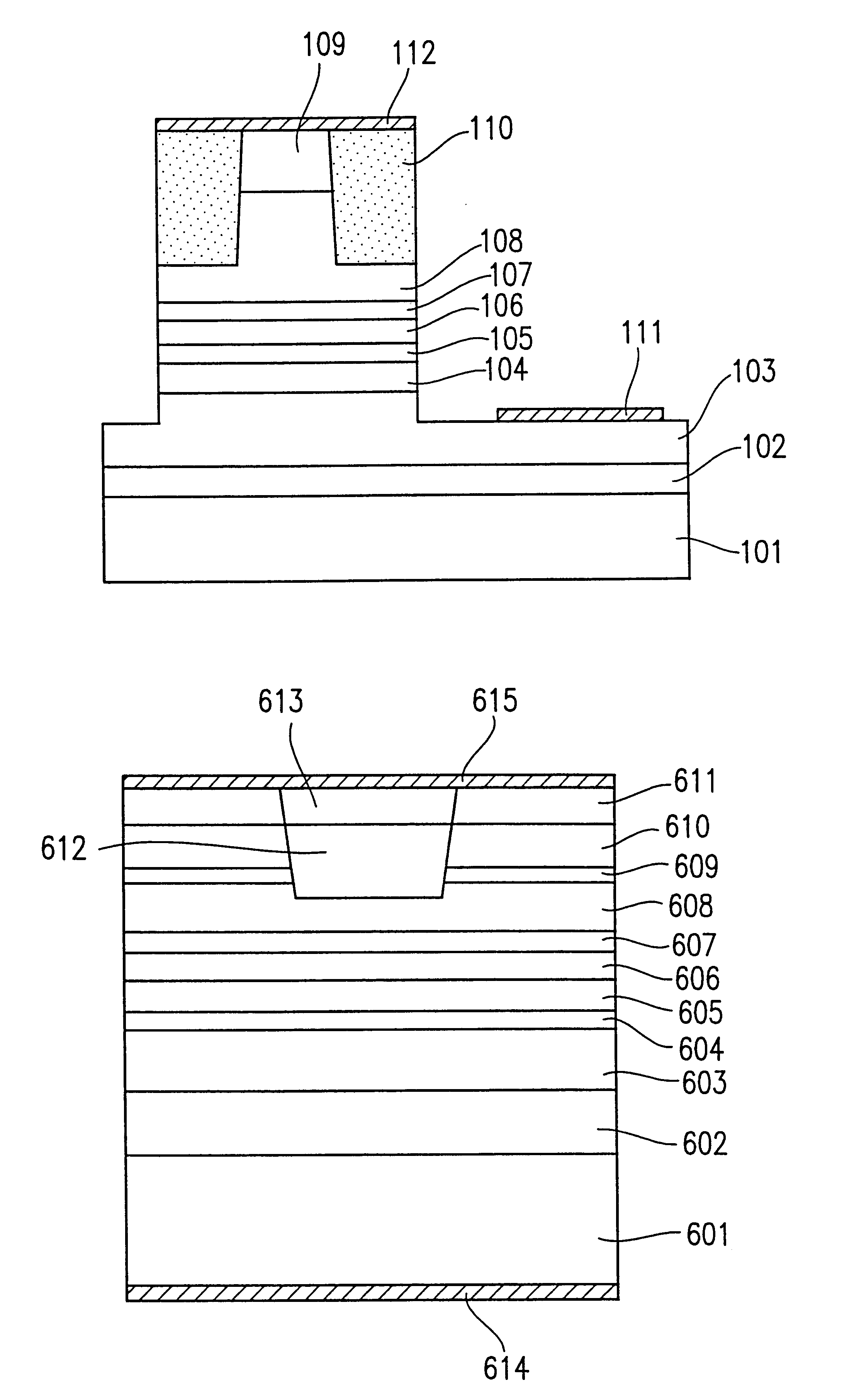
example 4

FIG. 10 is a schematic view showing a cross-sectional structure of a semiconductor laser according to Example 4 of the present invention, and FIG. 11 is a schematic view showing fabrication steps of the laser. A laser diode of the present example is fabricated according to a process as follows.

First, an undoped GaN buffer layer 602 of 20 nm, an n-Al.sub.0.08 Ga.sub.0.92 N first cladding layer 603 of 1 .mu.m, an n-GaN light confining layer 604 of 0.1 .mu.m, an active layer 605 of InGaN-MQW structure, a p-Al.sub.0.2 Ga.sub.0.8 N evaporation preventing layer 606 of 0.05 .mu.m, a p-GaN light confining layer 607 of 0.1 .mu.m, and p-Al.sub.0.08 Ga.sub.0.92 N second cladding layer 608 of 0.2 .mu.m, an n-Al.sub.0.3 Ga.sub.0.7 N light reflecting layer 609 of 0.1 .mu.m, a p-Al.sub.0.08 Ga.sub.0.92 N third cladding layer 610 of 0.7 .mu.m, and a p-GaN contact layer 611 of 0.5 .mu.m are epitaxially grown on an n-GaN substrate 601 in a sequential manner by the MOCVD method (FIG. 11(a)).

Next, a ma...


PUM


Abstract

A compound semiconductor laser of a III group nitride semiconductor of the present invention includes a first cladding layer 104 of a first conduction type formed on a substrate 101, an active layer 106 formed on the first cladding layer, a second cladding layer 108 of a second conduction type formed on the active layer 106, and a buried layer 110 formed on the second cladding layer 108, the buried layer having an opening portion for constricting a current in a selected region of the active layer, wherein an upper portion of the second cladding layer 108 has a ridge portion, the ridge portion residing in the opening portion of the buried layer 110, and the buried layer 110 does not substantially absorb light output from the active layer 106, and the buried layer has a refractive index which is approximately identical with that of the second cladding layer 108.

Description

The present invention relates to a semiconductor laser formed of a III group nitride semiconductor.FIG. 1 is a schematic cross-sectional view showing a conventional ridge waveguide type III group nitride semiconductor laser. A semiconductor laser of FIG. 1 has a stack structure including a GaN buffer layer 202, an n-GaN contact layer 203, an n-GaN buffer layer 204, an n-AlGaN cladding layer 205, an n-GaN guiding layer 206, an InGaN-MQW active layer 207, a p-AlGaN cap, layer 208, a p-GaN guiding layer 209, a p-AlGaN cladding layer 210, and a p-GaN contact layer 211 on a sapphire substrate 201. Since the sapphire substrate is insulative, a portion of the stack structure is etched down to the n-type contact structure 203 in order to expose a region to which an n-type electrode is attached. Furthermore, a portion of a mesa structure is etched down to the p-type cladding layer 210 in order to form a ridge waveguide. In these processes, a dry etching method is employed, and an SiO.sub.2 p...

Claims


Application Information

Patent Timeline
Patent Type & Authority Patents(United States)
IPC IPC(8): H01S5/323H01S5/223H01S5/00H01S5/343H01S5/22
CPCB82Y20/00H01S5/2231H01S5/32341H01S5/2211H01S5/2214H01S5/2218H01S5/34333H01S5/30
Inventor TAKATANI, KUNIHIRO
Owner SHARP KK
Why Eureka
Try Eureka