Weighted mean calculation circuit

a calculation circuit and weighted mean technology, applied in computation using denominational number representation, measurement using ac-dc conversion, instruments, etc., can solve the problems of circuit complexity, power consumption and the occupation area of a chip in digital processing, and achieve the effect of small occupation area and low power consumption

Inactive Publication Date: 2003-08-26
LINEAR CELL DESIGN COJ
View PDF3 Cites 16 Cited by
  • Summary
  • Abstract
  • Description
  • Claims
  • Application Information

AI Technical Summary

Benefits of technology

It is therefore an object of the invention to provide a weighted mean calculation circuit in which output signals are not caused to have any offset with respect to input signals, and it is another object of the invention to provide a weighted mean calculation circuit that enables lower power consumption and a smaller occupation area than any of prior arts.
Also, since, in a prior art weighted mean calculation circuit, input capacitance to which an input signal voltage is applied was different from the feedback capacitance to obtain an output, it was necessary to adjust both the input capacitance value and feedback capacitance value with respect to alternation of the weighting. However, since the same capacitance is used for the input capacitance and feedback capacitance in the system according to the invention, it is sufficient to change the weighting only in the input capacitance value, and a circuit configuration that varies the weighting by controlling it from the outside by using software can be easily constructed. In addition, since no excessive feedback capacitance is provided, not only the layout area thereof can be reduced equivalent thereto, but also the bias current value of an inverting amplifier to charge and discharge the capacitance can be decreased, whereby the power consumption and the occupation area can be further decreased than in any of the prior art weighted mean calculation circuits.
In the present invention, it is preferable that the above-described inverting amplifier is a CMOS inverting amplifier including a first MOS transistor of a source-grounding type, a second MOS transistor of the same polarity, which is cascode-connected thereto, and a load type third MOS transistor of the polarity opposite thereto. If such an inverting amplifier composed of the first MOS transistor and second MOS transistor, which are cascode-connected, is used, the gain can be increased using only one stage of the inverting amplifier to enable a decrease in power consumption and simultaneously increase the operating rate.
Also, in a case where components of capacitance inputted with respect to one signal voltage is composed of a plurality of capacitors, it is preferable that the ratio of capacitance values are made into 2 to the power of J (J is the integral number) like 1:2:4:8, whereby it is possible to maximize the range of variation of the weighting with a slight number of control signals.

Problems solved by technology

However, as the number of signals for a calculation input is increased, such a problem arises, in which power consumption and the occupation area in a chip are increased in digital processing.
However, since it is necessary to change the capacitance of C0 to alter the capacitance of the capacitors C1 through Cn in the construction shown in FIG. 11, another problem arises, which makes the circuit complicated if such a system in which the weighting is changed by controlling it from the outside is used.

Method used


Image

  • Weighted mean calculation circuit
  • Weighted mean calculation circuit
  • Weighted mean calculation circuit

Examples


embodiment 1

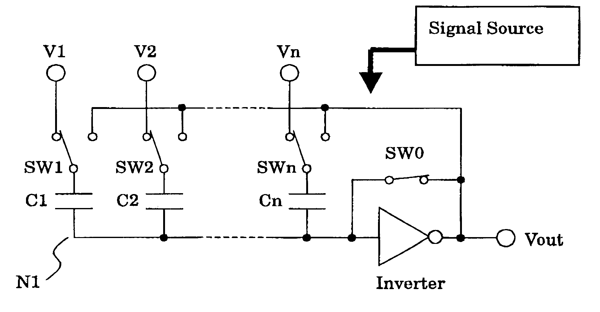
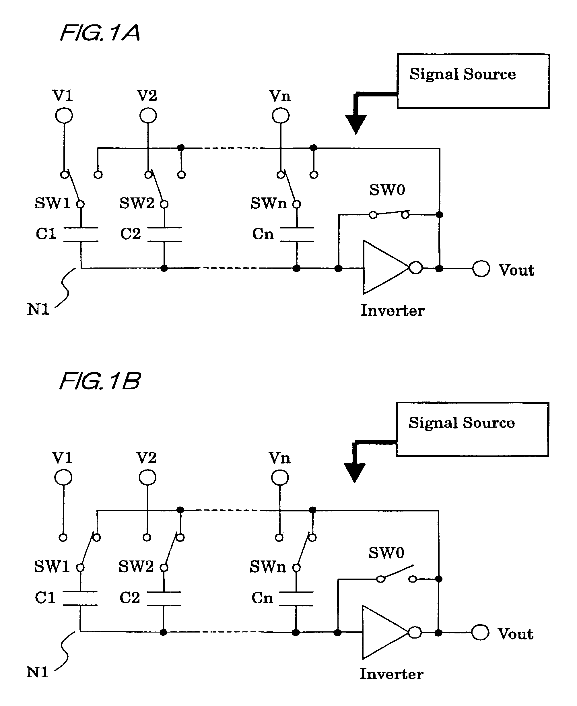
FIG. 1 shows the first embodiment to explain a weighted mean calculation circuit system according to the invention. FIG. 1A shows a connection when a signal input operation is carried out, FIG. 1B shows a connection when a signal output operation is carried out. The first embodiment includes an inverting amplifier (inverter); n capacitors C1 through Cn whose one end is connected to the input thereof; a switch SW0 that is provided to short-circuit between the input and output of the inverting amplifier; and switches SW1 through SWn to control whether the capacitor C1 through Cn are connected to input signal voltages V1 through Vn or the output terminal of the inverting amplifier.

In such a construction, as shown in FIG. 1A, when operating to input a signal, the SW0 is turned on and SW1 through SWn are connected to the input signal terminal side according to control signals of the signal source. At this time, since the input and output of the inverting amplifier are short-circuited by ...

embodiment 2

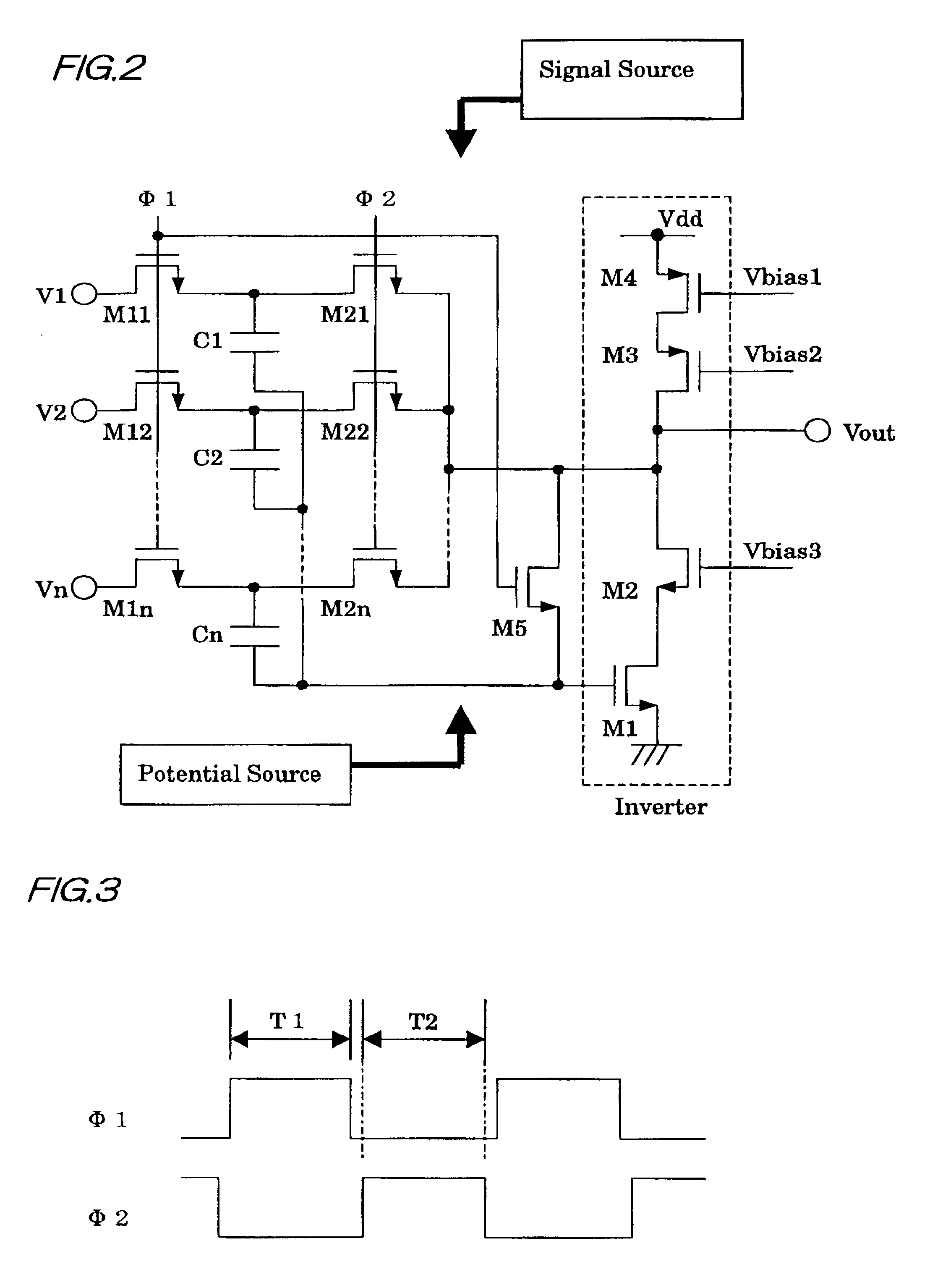
Next, with reference to FIG. 2, a description is given of the second embodiment consisting of a further detailed circuit configuration. As the inverting amplifier shown in FIG. 1, the circuit in FIG. 2 uses a CMOS inverting amplifier that includes a source-grounding type (common-source configuration) nMOS transistor M1, an nMOS transistor M2 that is cascode-connected to the drain of the transistor M1 and whose gate is provided with a constant voltage Vbias3, a pMOS transistor M4 that operates as a constant-current type load and whose gate is provided with a constant voltage Vbias1, and a pMOS transistor M3 that is cascode-connected to the drain of the transistor M4 and whose gate is provided with a fixed voltage Vbias2. Also, the switch SW0 is an nMOS transistor M5, and switches SW1 through SWn are two nMOS transistors of nMOS transistors M11 through M1n whose gate is provided with .PHI.1 from the signal source and nMOS transistors M21 through M2n whose gate is provided with .PHI.2 ...

embodiment 3

The weighted mean calculation circuits shown in FIG. 1 and FIG. 2 show a configuration in which input signals V1 through Vn are provided in parallel. However, a description is given of a weighted mean calculation circuit of serial data with reference to FIG. 4 that shows a configuration in which input signals are provided one after another in a time series, and FIG. 5 that shows a timing chart of its operation.

In FIG. 4, the configuration including an inverting amplifier (inverter), n capacitors C1 through Cn whose one end is connected to the input thereof, and a switch SW0 provided to short-circuit between the input and output of the inverting amplifier is identical to that in FIG. 1. Also, the other ends of the capacitors C1 through Cn are connected to a node N2, to which the respective capacitors are commonly connected, via the switches SW1 through SWn. These switches are different from the toggle switch in FIG. 1, but the switches are simple switches that select whether connecti...


PUM


Abstract

The present invention relates to a weighted mean calculation circuit that comprises an inverting amplifier; a plurality of capacitors C1 through Cn connected to the input terminal thereof; switches SW1 through SWn that connect the capacitors C1 through Cn to the input and output terminals of the inverting amplifier; and a switch SW0 that is provided between the input and output of the inverting amplifier. A signal voltage is applied to respective capacitors while making the SW0 conductive when inputting a signal, and the capacitors C1 through Cn are connected in parallel between the input and output of the inverting amplifier while making the SW0 non-conductive when outputting a signal, whereby an output signal Vout is read, and a weighted mean value output that does not include any offset and is normalized as a normal polarity output can be obtained.

Description

The present invention relates to a weighted mean calculation circuit for calculating a mean value by multiplying a plurality of signal voltages by weighting coefficients.Weighted mean calculations have widely been utilized for an image process in which spatial filtering is carried out on the basis of signals from an image input device, and for a transversal filter that carries out filtering with respect to time-series data for sampling serial data at a fixed interval. Normally, there are many cases where calculations are carried out after analog signals that are sampled with respect to space or time are converted to digital signals by an A / D converter. However, as the number of signals for a calculation input is increased, such a problem arises, in which power consumption and the occupation area in a chip are increased in digital processing.To the contrary, such a type has been proposed, in which a calculation system is employed with analog values for the purpose of a decrease in po...

Claims


Application Information

Patent Timeline
Patent Type & Authority Patents(United States)
IPC IPC(8): G06G7/14G06G7/00H03M1/74
CPCG06G7/14
Inventor UNO, MASAYUKI
Owner LINEAR CELL DESIGN COJ
Why Eureka
Try Eureka