Optical transmitter and optical signal transmitter

a technology of optical signals and optical modulators, applied in the field of optical transmitters, can solve problems such as chirping in particular, changing the characteristics of optical modulators, and yield in device manufacturing

Inactive Publication Date: 2004-06-29
OCLARO JAPAN INC
View PDF5 Cites 69 Cited by
  • Summary
  • Abstract
  • Description
  • Claims
  • Application Information

AI Technical Summary

Problems solved by technology

In this example, however, there is a problem in that the characteristics of the optical modulator are changed when the wavelength of the laser light led to the optical modulator is varied.
As for the above-mentioned first object of controlling the wavelength of a light source for a plurality of channels, one of the major problems is how to set the wavelength of a semiconductor laser device to be used as the light source at a standard value.
Therefore, there is a major problem in the yields in terms of device manufacturing.
This problem of wavelength control is a major obstacle to the achievement of smaller size and lower cost of an optical transmitter, and will also be a major object to further reduction in channel intervals and the increase in the number of channels in the future.
In addition, chirping in particular becomes a problem in the case of long-distance transmission.
In this case, however, the laser light output is reduced especially when the offset voltage is increased.
The variations are undesirable especially for long-distance transmission.
However, it is generally believed that in a semiconductor laser device, the carrier density varies as the driving current changes, thereby causing changes in the refractive index of the optical wave guide.
Then interference occurs between the optical signals including the above different wavelengths.

Method used


Image

  • Optical transmitter and optical signal transmitter
  • Optical transmitter and optical signal transmitter
  • Optical transmitter and optical signal transmitter

Examples


second embodiment

In this embodiment, wavelength variable type laser devices are used as a wavelength multiplexing laser array according to the present invention. This embodiment is an example of a new transmitter with a built-in optical modulator operating in a 1.55 .mu.m wavelength band. FIG. 10 is a plan view of a semiconductor optical device. FIG. 11 is a sectional view of the semiconductor optical device. The sectional view shows the schematically constitutional view of the components cross-sectioned along the optical path to facilitate understanding of the connection between each of the components and the optical wave guide or the like. Therefore, FIG. 11 is not an accurate sectional view.

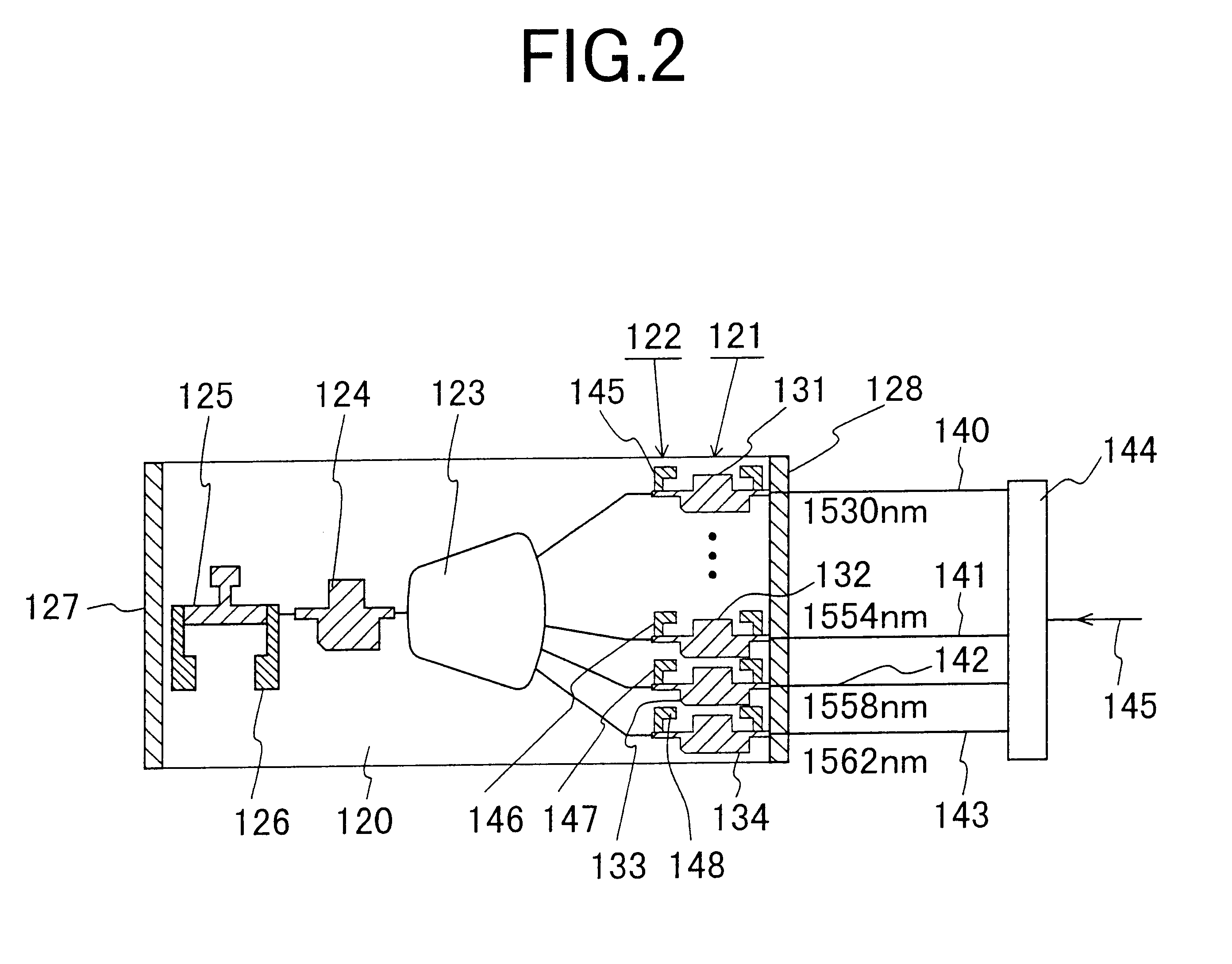
FIG. 10 shows the basic configuration of the semiconductor optical device 201 of the second embodiment. Light from each laser device of a multiple wavelength distributed feedback laser array 202 is led to a optical multiplexer 204. In FIG. 10, the plurality of laser devices and temperature control means for th...

third embodiment

This embodiment is an example of a semiconductor optical device with a DBR (Distributed Bragg Reflection) type laser. FIG. 13 is a plan view of an example of a new transmitter with a built-in optical modulator according to the present invention. FIG. 14 is a sectional view of the transmitter. The apparatus in this embodiment operates in a 1.55 .mu.m wavelength band.

In the semiconductor optical device of the present embodiment, a first distributed reflector 304 region, a phase adjustment layer 306 region, an active layer region 302 for laser oscillation, a second distributed reflector 303 region, and an optical modulator 308 region are optically connected to each other. Also, in this embodiment, a temperature control means 307 is provided for the optical modulator 308. A specific example of the temperature control means 307 is a heater. Low-reflection planes 309 and 310 are formed on both end surfaces of the semiconductor optical device containing the above optical means.

Each laminat...

fourth embodiment

This embodiment is an example including a compound resonator type laser using an array wave guide diffraction grating. FIG. 15 shows a new transmitter with a built-in optical modulator operating in a 1.55 .mu.m wavelength band, which is produced according to the present invention. FIG. 15 is a plan arrangement view of the semiconductor optical device with a compound resonator type laser using an array wave guide diffraction grating. FIG. 16 is a sectional view of the semiconductor optical device. Incidentally, the sectional view shows the schematically constitutional view of the components cross-sectioned along the optical path to facilitate understanding of the connection between each of the components and the optical wave guide or the like. Therefore, FIG. 16 is not an accurate sectional view.

The laser resonator of the semiconductor optical device comprises a laser active region 411, a distributed reflector 413, a phase adjuster 412, and an array wave guide diffraction grating 415...


PUM

PropertyMeasurementUnit
wavelengthaaaaaaaaaa
frequencyaaaaaaaaaa
thicknessaaaaaaaaaa

Abstract

The optical transmitter includes a semiconductor laser device, and an optical modulator region optically connected to the semiconductor laser device and having the function of modulating the output light from the semiconductor laser device. The operating temperature of the optical modulator region is changed without changing the oscillation wavelength of the semiconductor laser device.

Description

1. Field of the InventionThe present invention relates to an optical transmitter and more particularly to an optical transmitter a wavelength multiplexing optical communication system and an optical network using a plurality of pieces of signal light.2. Related ArtWavelength multiplexing optical communication, which transmits an optical signal with a plurality of wavelengths along the same optical transmission line, is an important technology for achieving higher performance and lower cost of communication technology and optical information processing technology. A first major object from this point of view is to control the wavelength of a light source for a plurality of channels, and a second major object is to provide an optical modulation means for achieving rapid optical modulation.Controlling the wavelength of a light source for a plurality of channels in a wavelength multiplexing optical communication system is one of the most important techniques. The wavelength c)r frequenc...

Claims


Application Information

Patent Timeline
Patent Type & Authority Patents(United States)
IPC IPC(8): H04B10/152H04B10/155H01S5/026B82Y20/00G02B6/12G02B6/42G02F1/025H01S5/50H04B10/032H04B10/079H04B10/293H04B10/564H04B10/572
CPCH04B10/504H04B10/572G02F1/0121G02F1/017G02F1/2257
Inventor AOKI, MASAHIRO
Owner OCLARO JAPAN INC
Why Eureka
Try Eureka