Thin-film EL device, and its fabrication process

a thin-film el and fabrication process technology, applied in the manufacture of electrode systems, electric discharge tubes/lamps, discharge tubes luminescent screens, etc., can solve the problems of limited use, structural problems such as unsolved thin-film el devices, and difficulty in reducing to nil steps

Inactive Publication Date: 2004-10-26
IFIRE IP CORP
View PDF24 Cites 0 Cited by
  • Summary
  • Abstract
  • Description
  • Claims
  • Application Information

AI Technical Summary

Benefits of technology

From the foregoing, the advantages of the invention can be understood.The present invention a solution to all problems with the prior art viz., an fatal defect to display devices, which, when an insulator layer is made up of a thin film, results from destruction of a light-emitting layer due to a local dielectric strength decrease ascribable to defects in the insulator layer; poor light emission properties which, when a thick-film dielectric layer made up of ceramics is used, result from defects on the surface of the dielectric layer, the fact that the dielectric layer is porous, and the asperity configuration of the surface of the dielectric layer; cost increases due to the addition of a difficult-to-perform step, i.e., the step of polishing the surface of the thick-film dielectric layer, and further cost increases due to the addition of a sol-gel step; and limitations imposed on the selection of substrate and electrode layer materials thanks to the firing temperature for the thick-film dielectric layer. Thus, the present invention provides a thin-film EL device and its fabrication process without incurring any cost increase. The thin-film EL device of the invention allows restrictions on the selection of substrate materials to be removed, and so makes it possible to use glass substrates which are inexpensive and can be easily processed to a large area, and can rely on a quick-and-easy process to make correction for non-flat portions of a dielectric layer due to an electrode layer, and dust, etc. resulting from process steps, thereby preventing any dielectric strength decrease. In addition, the thin-film EL device of the invention ensures high display quality by virtue of the satisfactory flatness of the surface of the dielectric layer.

Problems solved by technology

Known for long, the dispersion type EL device has the advantage of ease of fabrication; however, it has only limited use thanks to low luminance and short service life.
However, a structural problem with such a thin-film EL device remains unsolved.
The problem is that since the insulator layers are each formed of a thin film, it is difficult to reduce to nil steps at the edges of the pattern of the transparent electrode, which occur when a large area display is fabricated, and defects in the thin-film insulators, which are caused by dust, etc. occurring in the process of display production, resulting in a destruction of the light-emitting layer due to a local dielectric strength drop.
Such defects offer a fatal problem to display devices, and produce a bottleneck in the wide practical use of thin-film EL devices in a large-area display system, in contrast to liquid crystal displays or plasma displays.
The use of this thick-film dielectric layer leads to another problem that the effective voltage applied to the light-emitting layer drops.
However, it is still difficult to sufficiently smooth down the surface of a dielectric layer fabricated by an ordinary thick-film process.
For this reason, the sintering of the thick-film dielectric layer does not proceed to a sufficient level, yielding an essentially porous layer.
Since the process of close packing proceeds through a ceramic solid phase reaction of powders having a certain particle size distribution, sintering abnormalities such as abnormal crystal grain growth and macropores are likely to occur.
This makes it impossible to effectively apply an electric field to the portion of the light-emitting layer formed on a non-flat portion of the substrate, resulting in problems such as a decrease in the effective light-emitting area, and a light emission luminance decrease due to a local dielectric breakdown of the light-emitting layer, which is caused by local non-uniform thicknesses.
Furthermore, locally large thickness fluctuations cause the strength of an electric field applied to the light-emitting layer to vary too locally largely to obtain any definite light emission voltage threshold.
However, the polishing of a large-area substrate for display or other purposes is technically difficult to achieve, and is a factor for cost increases as well.
The addition of the sol-gel step is another factor for cost increases.
When a thick-film dielectric layer has abnormal sintered spots which may give rise to asperities too large for removal by polishing, yields drop because they cannot be removed even by the addition of the sol-gel step.
It is thus very difficult to use a thick-film dielectric material to form a light emission defect-free dielectric layer at low cost.
In consideration of heat resistance and a reactivity problem with respect to the dielectric layer, the substrate used for the formation of such a thick-film dielectric layer is limited to alumina or zirconia ceramic substrate; it is difficult to rely on inexpensive glass substrates.
The substrate meeting such conditions is obtained only with much technical difficulty, and is yet another factor for cost increases.
This, too, is a factor for cost increases.
(1) an fatal defect to display devices, which, when an insulator layer is made up of a thin film, results from destruction of a light-emitting layer due to a local dielectric strength decrease ascribable to defects in the insulator layer,
(2) poor light emission properties which, when a thick-film dielectric layer made up of ceramics is used, result from defects on the surface of the dielectric layer, the fact that the dielectric layer is porous, and the asperity configuration of the surface of the dielectric layer,
(3) cost increases due to the addition of a difficult-to-perform step, i.e., the step of polishing the surface of the thick-film dielectric layer, and further cost increases due to the addition of a sol-gel step, and
(4) limitations imposed on the selection of substrate and electrode layer materials thanks to the firing temperature for the thick-film dielectric layer.

Method used


Image

  • Thin-film EL device, and its fabrication process
  • Thin-film EL device, and its fabrication process
  • Thin-film EL device, and its fabrication process

Examples


example 1

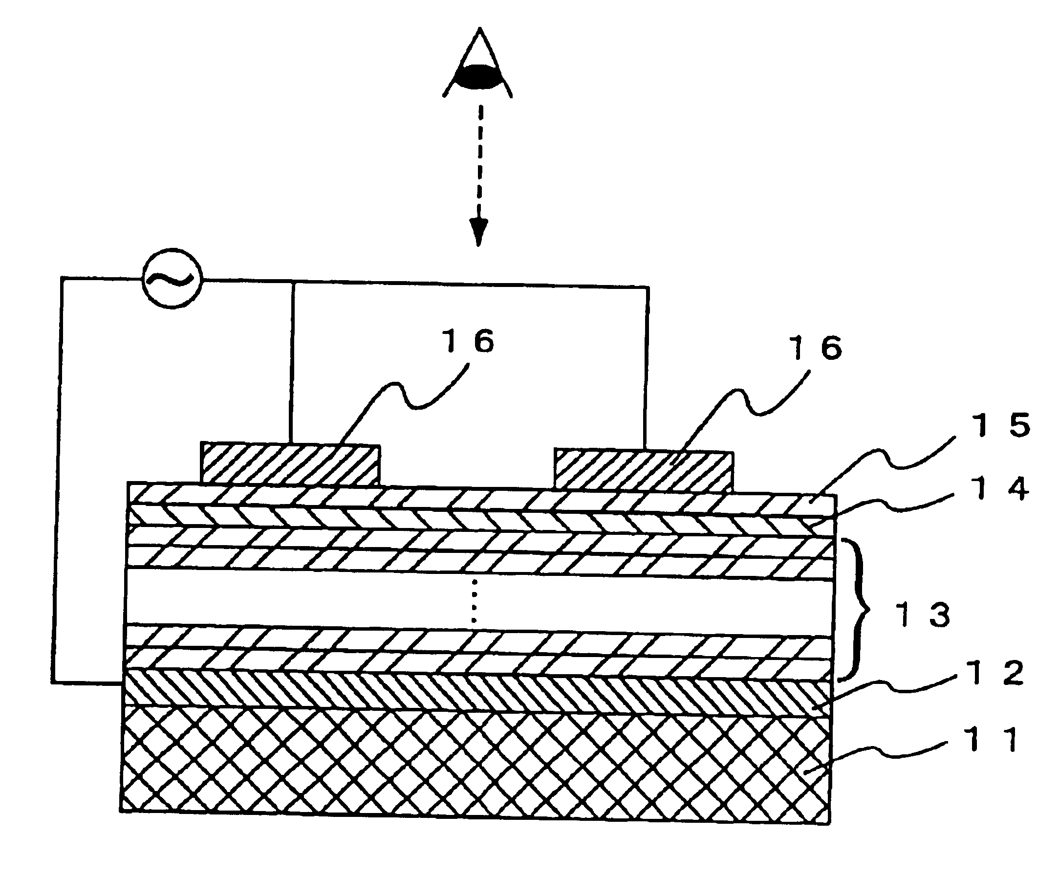
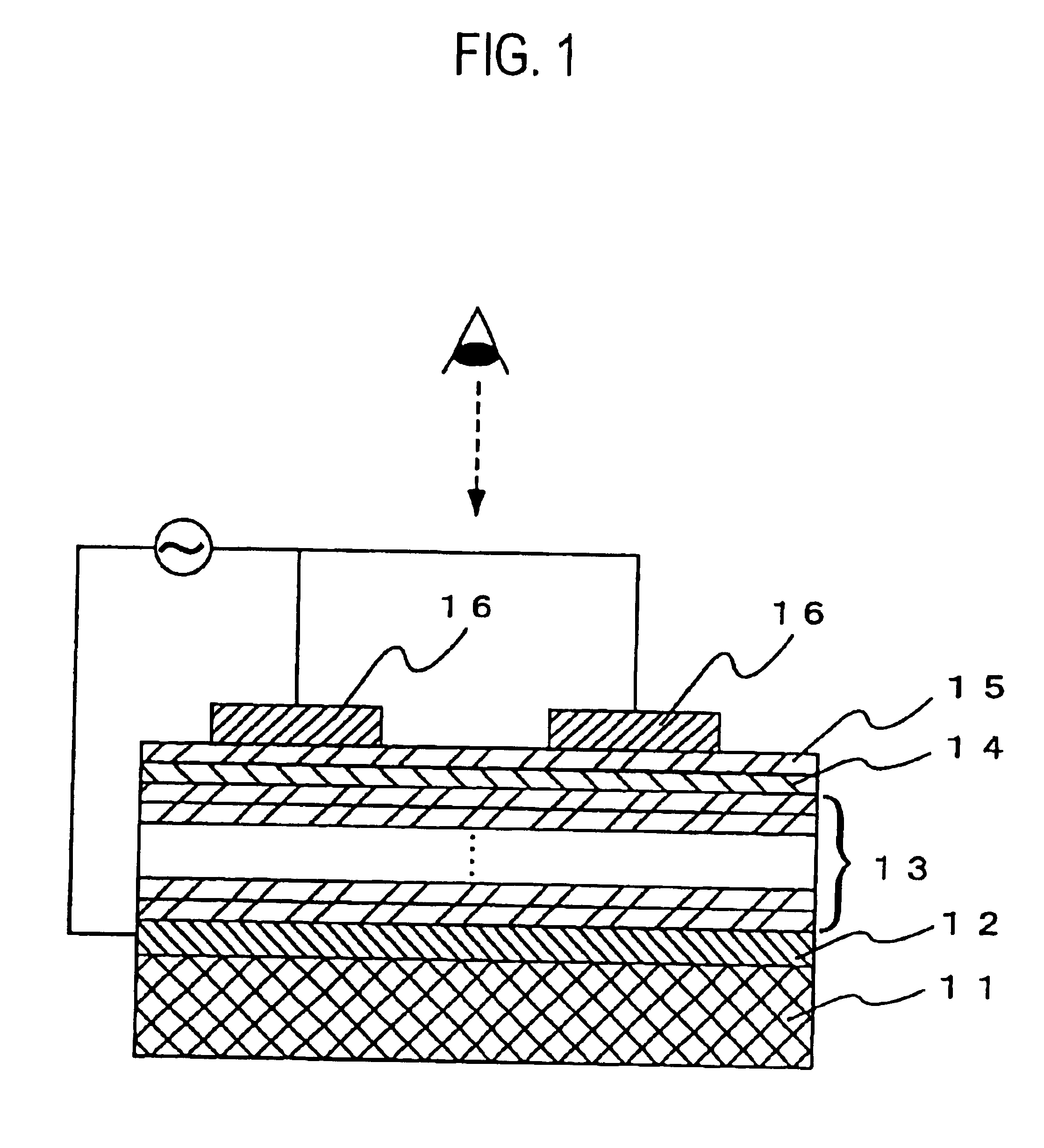
A 1 .mu.m thick Au thin film with trace additives added thereto was formed by sputtering on a surface polished alumina substrate of 99.6% purity, and heat treated at 700.degree. C. for stabilization. Using a photoetching process, this Au thin film was patterned in a striped arrangement comprising a number of stripes having a width of 300 .mu.m and a space of 30 .mu.m.

A dielectric layer was formed on the substrate using the solution coating-and-firing step. The dielectric layer was formed by repeating given times the solution coating-and-firing step wherein a sol-gel solution prepared as mentioned below was spin coated as a PZT precursor solution on the substrate and fired at 700.degree. C. for 15 minutes.

To prepare a basic sol-gel solution, 8.49 grams of lead acetate trihydrate and 4.17 grams of 1,3-propanediol were heated under agitation for about 2 hours to obtain a transparent solution. Apart from this, 3.70 grams of a 70 wt % 1-propanol solution of zirconium.normal propoxide and...

example 2

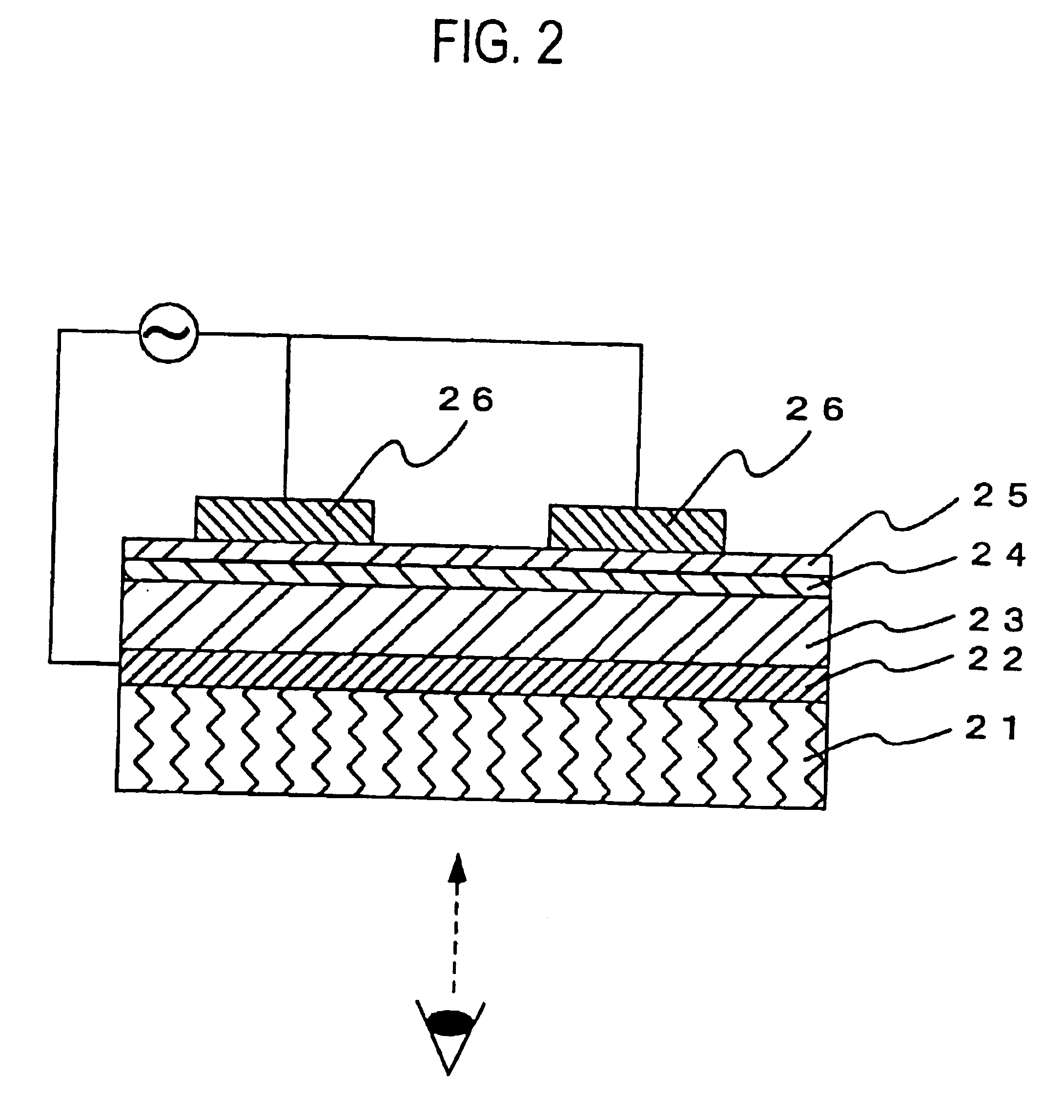
A soda lime-based high heat-resistant glass substrate (having a softening point of 820.degree. C.) was provided. A 0.5 .mu.m thick Ag / Pd / Cu thin film as a thin-film lower electrode layer was formed by sputtering on this substrate, and then heat treated at 700.degree. C. for stabilization. A pattern comprising a number of stripes of 500 .mu.m in width and 50 .mu.m in space was formed by patterning the thin-film lower electrode layer using a photoetching process.

A dielectric layer was formed on the substrate using the solution coating-and-firing step. The dielectric layer was formed by repeating given times the solution coating-and-firing step wherein a sol-gel solution prepared as mentioned below was dip coated as a BaTiO.sub.3 precursor solution on the substrate and fired at the maximum temperature of 700.degree. C. for 10 minutes. The then thickness of each sub-layer in the dielectric layer was 1.5 .mu.m.

To prepare the BaTiO.sub.3 precursor solution, PVP (polyvinyl pyrrolidone) hav...


PUM


Abstract

The invention has for its object to provide, without incurring any cost increase, a thin-film EL device in which a dielectric layer is corrected for non-flat portions to have a smooth surface, thereby ensuring enhanced display quality, and its fabrication process. This object is achieved by the provision of a thin-film EL device having at least a structure comprising an electrically insulating substrate (11), a lower electrode layer (12) stacked on the substrate according to a given pattern, a multilayer dielectric layer (13) formed thereon by repeating a solution coating-and-firing step plural times, and a light-emitting layer (14), a thin-film insulator layer (15) and a transparent electrode layer (16) stacked on the dielectric layer. The multilayer dielectric layer has a thickness of at least four times as large as a thickness of the electrode layer and 4 mum to 16 mum inclusive. The fabrication process is also provided.

Description

1. Art FieldThis invention relates to a thin-film EL device having at least a structure comprising an electrically insulating substrate, a patterned electrode layer stacked on the substrate, and a dielectric layer, a light-emitting layer and a transparent electrode layer stacked on the electrode layer.2. Background ArtEL devices are now practically used in the form of backlights for liquid crystal displays (LCDs) and watches. An EL device works on a phenomenon in which a substance emits light at an applied electric field, viz., an electro-luminescence (EL) phenomenon. The EL device is broken down into two types, one referred to as a dispersion type EL device having a structure wherein electrode layers are provided on the upper and lower sides of a dispersion with light-emitting powders dispersed in an organic material or porcelain enamel, and another as a thin-film EL device using a thin-film light-emitting substance provided on an electrically insulating substrate and interposed be...

Claims


Application Information

Patent Timeline
Patent Type & Authority Patents(United States)
IPC IPC(8): H05B33/10H05B33/22
CPCH05B33/22H05B33/10
Inventor SHIRAKAWA, YUKIHIKO
Owner IFIRE IP CORP
Why Eureka
Try Eureka