Surface planarization of thin silicon films during and after processing by the sequential lateral solidification method

a technology of surface planarization and thin silicon, applied in the direction of crystal growth process, manufacturing tools, coatings, etc., can solve the problems of low manufacturing yield, non-uniform device, and difficulty in generating polycrystalline or single crystal silicon

Inactive Publication Date: 2004-12-14
THE TRUSTEES OF COLUMBIA UNIV IN THE CITY OF NEW YORK
View PDF9 Cites 79 Cited by
  • Summary
  • Abstract
  • Description
  • Claims
  • Application Information

AI Technical Summary

Problems solved by technology

The use of conventional excimer laser annealing technology to generate polycrystalline or single crystal silicon is problematic for several reasons.
First, the silicon generated in the process is typically small grained, of a random microstructure, and / or has non-uniform grain sizes, which result in poor and non-uniform devices that lead to low manufacturing yield.
Also, these processes generally require a controlled atmosphere and preheating of the amorphous silicon sample, which lead to a further reduction in throughput rates.
Finally, the fabricated films generally exhibit an unacceptable degree of surface roughness that can be problematic for performance of microelectronic devices.

Method used


Image

  • Surface planarization of thin silicon films during and after processing by the sequential lateral solidification method
  • Surface planarization of thin silicon films during and after processing by the sequential lateral solidification method
  • Surface planarization of thin silicon films during and after processing by the sequential lateral solidification method

Examples


first embodiment

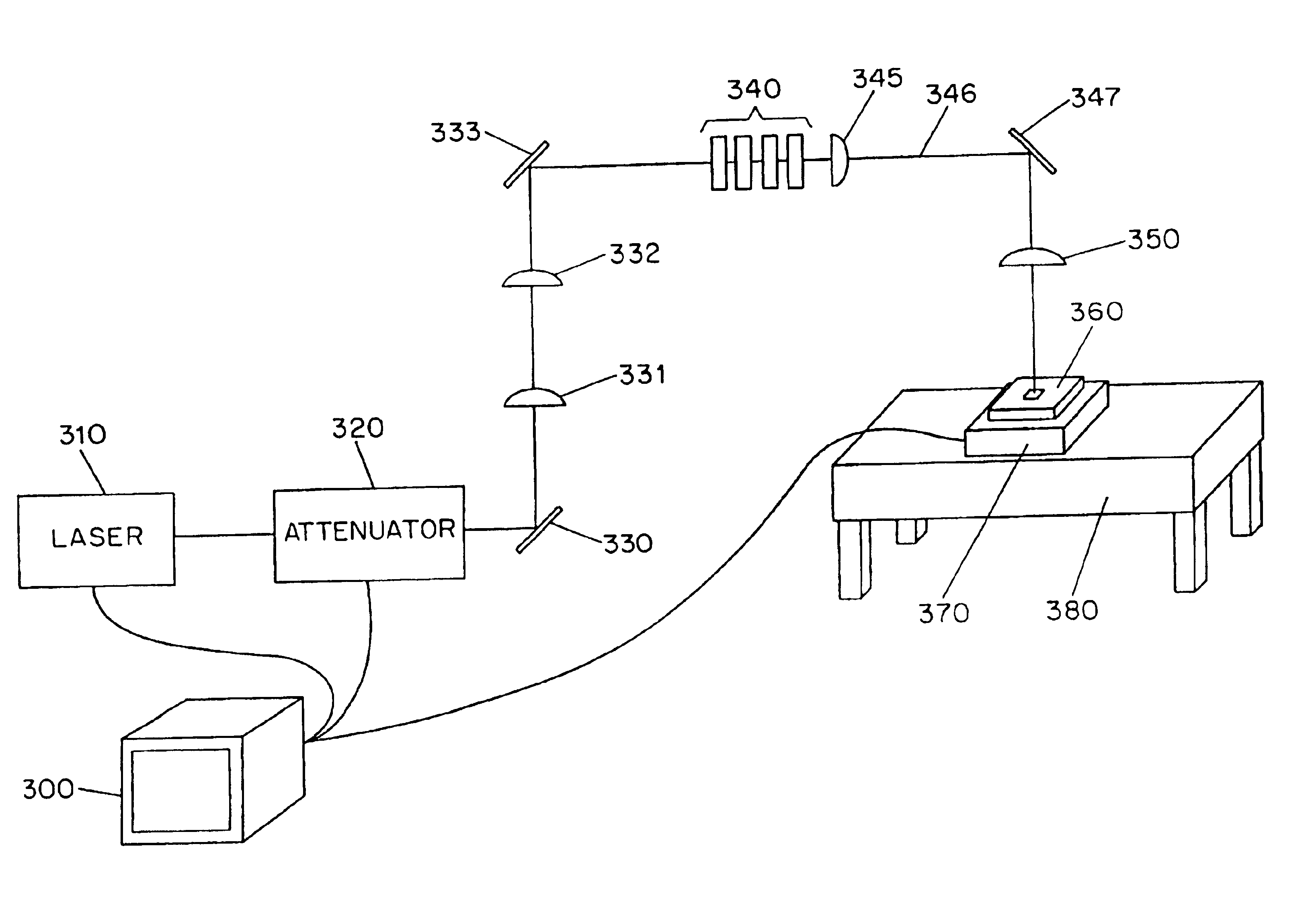
Referring to FIGS. 3 and 4, the present invention will now be described. FIG. 3 illustrates a post processing system embodiment for planarizing polycrystalline and single crystal thin film semiconductors produced by the sequential lateral solidification process. The system includes an excimer laser 310, beam attenuator and shutter 320, reflecting plate 330, telescoping lenses 331, 332, reflecting plate 333, beam homogenizer 340, condensing lens 345, reflecting plate 347, field lense 350, sample 360, sample translation stage 370, optical table 380, and managing computer 300. A preferred laser 310, attenuator 320, telescoping lenses 332, 332, homogenizer 340, and sample translation stage 370 that is movable in two orthogonal directions are each described in the co-pending patent application Ser. No. 09 / 390,537. The table 380 may be as described in that patent document, or may be an ordinary table. It is preferable that the homogenized beam 346 be shaped with a tophat profile in both t...

second embodiment

Referring next to FIG. 8, the present invention will now be described. In this embodiment, the surface of silicon thin film is kept planarized through the employment of a rigid cap layer during the sequential lateral solidification process. Thus, FIG. 8 shows a thin silicon sample formed of an approximately 50-200 nm thick amorphous silicon layer 810 deposited on a silicon oxide base layer 820. The sample is capped with a thick second silicon oxide layer 820, approximately 2 microns thick, which is substantially rigid. The cap layer must be sufficiently thick to withstand the contractions and expansions during melting and resolidification of the silicon layer during the sequential lateral solidification process.

The sample with cap layer 830 are then used in place of sample 170 in the lateral solidification process, a complete description of which is contained in the above mentioned patent application Ser. No. 09 / 390,537. After such processing, the cap layer 830 is removed from the s...


PUM

PropertyMeasurementUnit
melt thresholdaaaaaaaaaa
widthaaaaaaaaaa
widthaaaaaaaaaa

Abstract

Systems and methods for reducing a surface roughness of a polycrystalline or single crystal thin film produced by the sequential lateral solidification process are disclosed. In one arrangement, the system includes an excimer laser (110) for generating a plurality of excimer laser pulses of a predetermined fluence, an energy density modulator (120) for controllably modulating the fluence of the excimer laser pulses such that the fluence is below that which is required to completely melt the thin film, a beam homoginizer (144) for homoginizing modulated laser pulses in a predetermined plane, a sample stage (170) for receiving homoginized laser pulses to effect melting of portions of the polycrystalline or single crystal thin film corresponding to the laser pulses, translating means for controllably translating a relative position of the sample stage (170) with respect to the laser pulses, and a computer (110) for coordinating the excimer pulse generation and fluence modulation with the relative positions of the sample stage (170) to thereby process the polycrystalline or single crystal thin film by sequential translation of the sample stage (170) relative to the laser pulses.

Description

I. Field of the InventionThe present invention relates to techniques for semiconductor processing, and more particularly to semiconductor processing which may be performed at low temperatures.II. Description of the Related ArtIn the field of semiconductor processing, there have been several attempts to use lasers to convert thin amorphous silicon films into polycrystalline films. An overview of conventional excimer laser annealing technology is presented by James Im et al. in "Crystalline Si Films for Integrated Active-Matrix Liquid-Crystal Displays," 11 MRS Bulletin 39 (19%). In systems used for carrying out excimer laser annealing, an excimer laser beam is shaped into a long beam which is typically up to 30 cm long and 500 micrometers or greater in width. The shaped beam is scanned over a sample of amorphous silicon to facilitate melting thereof and the formation of polycrystalline silicon upon resolidification of the sample.The use of conventional excimer laser annealing technolo...

Claims


Application Information

Patent Timeline
Patent Type & Authority Patents(United States)
IPC IPC(8): B23K26/06H01L21/00H01L21/20H01L21/02B23K26/00H01L21/302H01L21/321
CPCB23K26/0075B23K26/06B23K26/063B23K26/0656B23K26/0853H01L21/2026H01L21/302H01L21/32115H01L21/67253Y10S438/942B23K2201/40B23K26/0622B23K26/066B23K26/3576B23K2101/40H01L21/02532H01L21/02678H01L21/02686H01L21/02691
Inventor IM, JAMES S.SPOSILI, ROBERT S.CROWDER, MARK A.
Owner THE TRUSTEES OF COLUMBIA UNIV IN THE CITY OF NEW YORK
Why Eureka
Try Eureka