Laser ablation method for patterning a thin film layer

a thin film layer and laser ablation technology, applied in the direction of identification means, instruments, manufacturing tools, etc., can solve the problems of increasing power consumption, reducing display reliability, and not achieving the phosphor luminescence and colour needed to be fully competitiv

Inactive Publication Date: 2005-01-04
IFIRE IP CORP
View PDF7 Cites 11 Cited by
  • Summary
  • Abstract
  • Description
  • Claims
  • Application Information

AI Technical Summary

Benefits of technology

According to an aspect of the invention, there is provided a laser ablation method for patterning a thin film phosphor layer of a thick film dielectric electroluminescent display having other layers, the method comprising selecting a wavelength of laser radiation, a laser pulse length, a laser energy density and a sufficient number of laser pulses to pattern the thin film phosphor layer without substantial ablation of or damage to other layers, whereby the wavelength of laser radiation is such that the laser radiation is substantially absorbed by the thin film phosphor layer with minimal absorption by other layers, the laser pulse length is sufficiently short that during the duration of the laser pulse there is minimal heat flow from the thin film phosphor layer to other layers, and the laser energy density and the sufficient number of laser pulses is sufficiently high that energy is deposited in the thin film phosphor layer, whereby the entir

Problems solved by technology

Unfortunately, thick film electroluminescent displays have not achieved the phosphor luminescence and colour needed to be fully competitive with cathode ray tube (CRT) displays, particularly with recent trends in CRT specifications to higher luminescence and higher colour.
Some improvement has been realized by increasing the operating voltage of the displays, but this increases the power consumption and decreases the reliability of the displays.
The problem,

Method used


Image

  • Laser ablation method for patterning a thin film layer
  • Laser ablation method for patterning a thin film layer

Examples


example 1

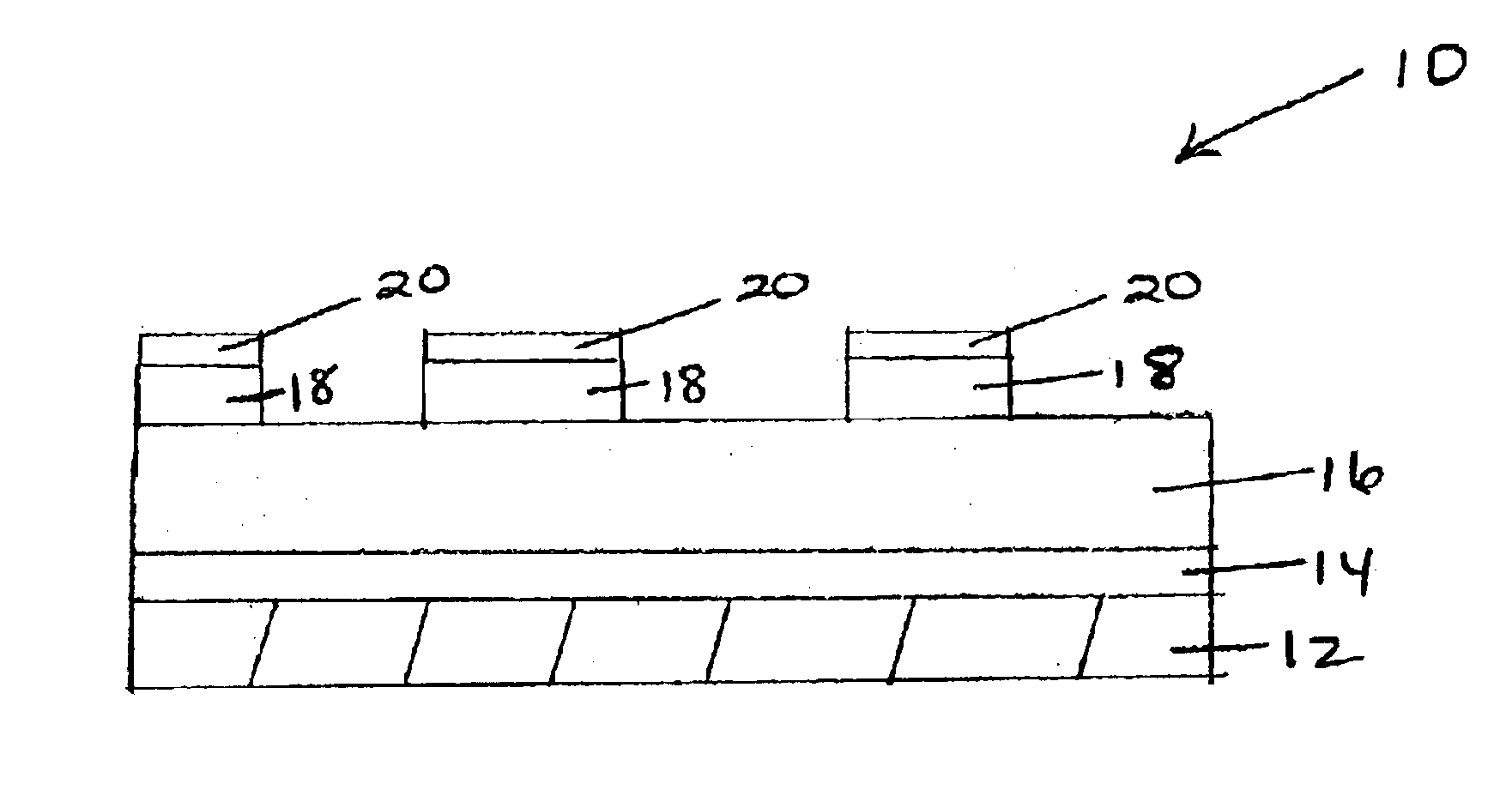
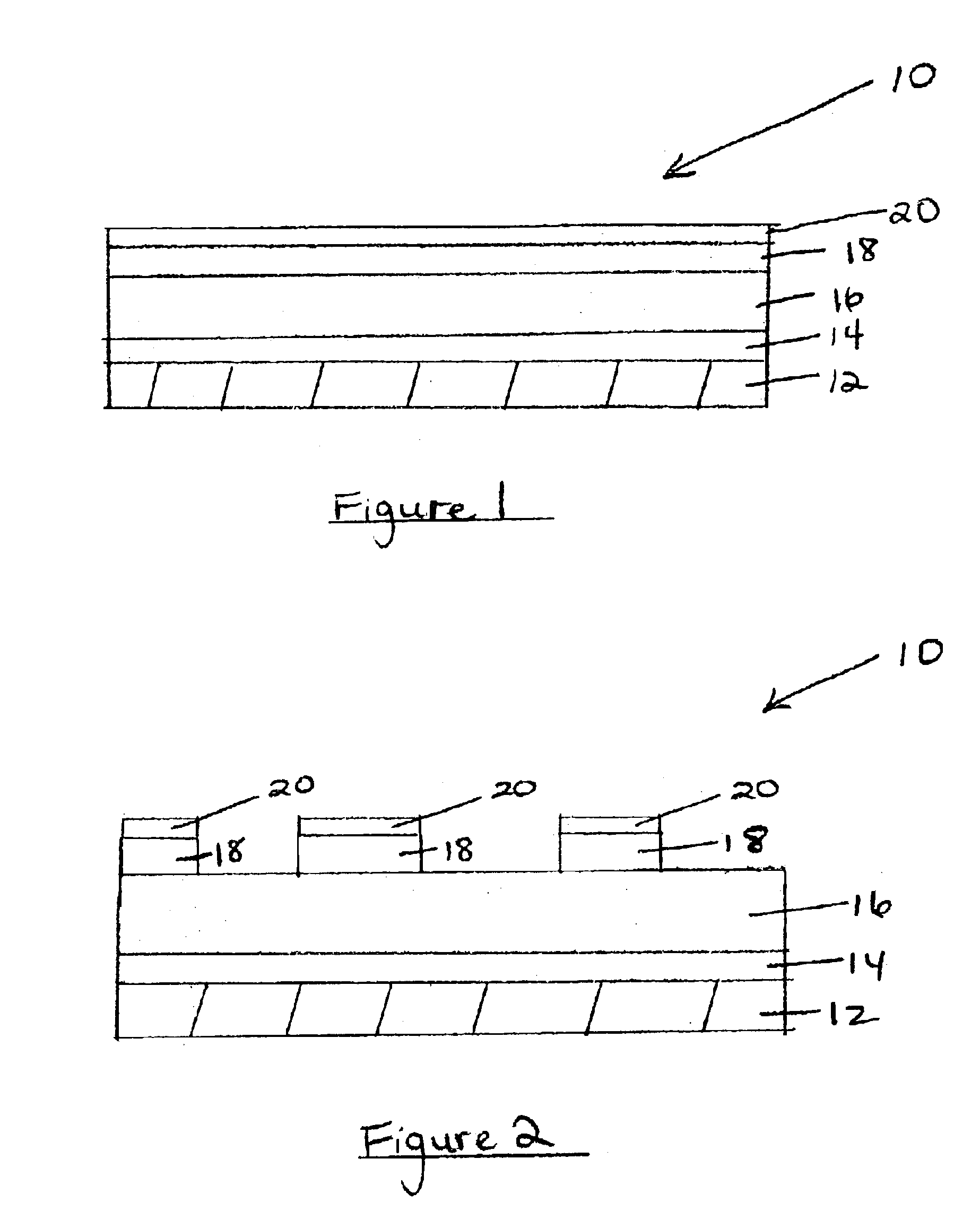
A thick film electroluminescent display was made as described above, wherein the europium activated magnesium barium thioaluminate phosphor film layer is about 270 nanometers thick and the underlying layer of barium titanate is about 15 nanometers thick. To the top of the phosphor film layer was sputtered a protective layer of alumina, which is about 45 nanometers thick, followed by a layer of indium tin oxide, which is about 100 nanometers thick. The indium tin oxide acts as both an electrode and protective layer for the display.

The phosphor film layer together with the overlying layers were ablated using an excimer laser having a laser wavelength of 248 nanometers, a laser energy density of 1.5 joules per square centimeter and a laser pulse repetition rate to give a pulse every 26 micrometers along the ablation path.

This resulted in a phosphor film layer that could be independently illuminated by applying a voltage between the gold electrode and the indium tin oxide layer. The lum...

example 2

A display similar to that of Example 1 was fabricated, except that the laser energy density was higher at 2 joules per square centimeter and the laser pulse repetition rate was lower so that there was a pulse applied every 52 micrometers along the ablation trench.

This display performed similarly to that of Example 1.


PUM

PropertyMeasurementUnit
Timeaaaaaaaaaa
Timeaaaaaaaaaa
Thicknessaaaaaaaaaa

Abstract

The invention relates to a laser ablation method for patterning thin film layers for thick dielectric electroluminescent displays without substantial ablation of or damage to any other layers. Typically, the thin film layers are phosphor layers. The laser ablation method for patterning a thin film phosphor layer of a thick dielectric electroluminescent display includes selecting a wavelength of laser radiation, a laser pulse length, a laser energy density and a sufficient number of laser pulses to pattern the thin film phosphor layer without substantial ablation of or damage to other layers, whereby the wavelength of laser radiation is such that the laser radiation is substantially absorbed by the thin film phosphor layer with minimal absorption by other layers, the laser pulse length is sufficiently short that during the duration of the laser pulse there is minimal heat flow from the thin film phosphor layer to other layers, and the laser energy density and the sufficient number of laser pulses is sufficiently high that energy is deposited in the thin film phosphor layer, whereby the entire thickness of at least a portion of the thin film phosphor layer is ablated.

Description

FIELD OF THE INVENTIONThe present invention relates to a laser ablation method for patterning thin film layers for thick dielectric electroluminescent displays. More particularly, the invention relates to a laser ablation method for patterning thin film phosphor layers without substantial ablation of or damage to any other layers.BACKGROUND OF THE INVENTIONThick film dielectric electroluminescent displays (TDEL) provide a great advance in flat panel display technology. TDEL displays comprise a basic structure of, in sequence, a substrate, an electrically conductive film layer to form the lower electrode, a thick dielectric film layer, a phosphor film deposited on the thick film layer, and an optically transparent but electrically conductive film to form the upper electrode in the structure.Various aspects of manufacturing TDEL displays are described in Applicant's co-pending U.S. patent application Ser. No. 09 / 747,315 filed Dec. 22, 2000; Ser. No. 09 / 761,971 filed Jan. 17, 2001; Ser...

Claims


Application Information

Patent Timeline
IPC IPC(8): B23K26/40B23K26/00H05B33/10H05B33/12B23K26/12B23K26/36B23K26/38B23K101/36G09F9/00H01L51/00H05B33/14H05B33/28
CPCB23K26/0045B23K26/0048B23K26/38B23K26/401B23K26/408H05B33/12B23K26/409B23K26/4095H01L51/0005H05B33/10B23K26/4085B23K26/0006B23K26/40B23K2101/35B23K2103/172B23K2103/50B23K2103/52H10K71/135
Inventor LOVELL, DAVEHUNT, TERRY
Owner IFIRE IP CORP
Why Eureka
Try Eureka